


fig1
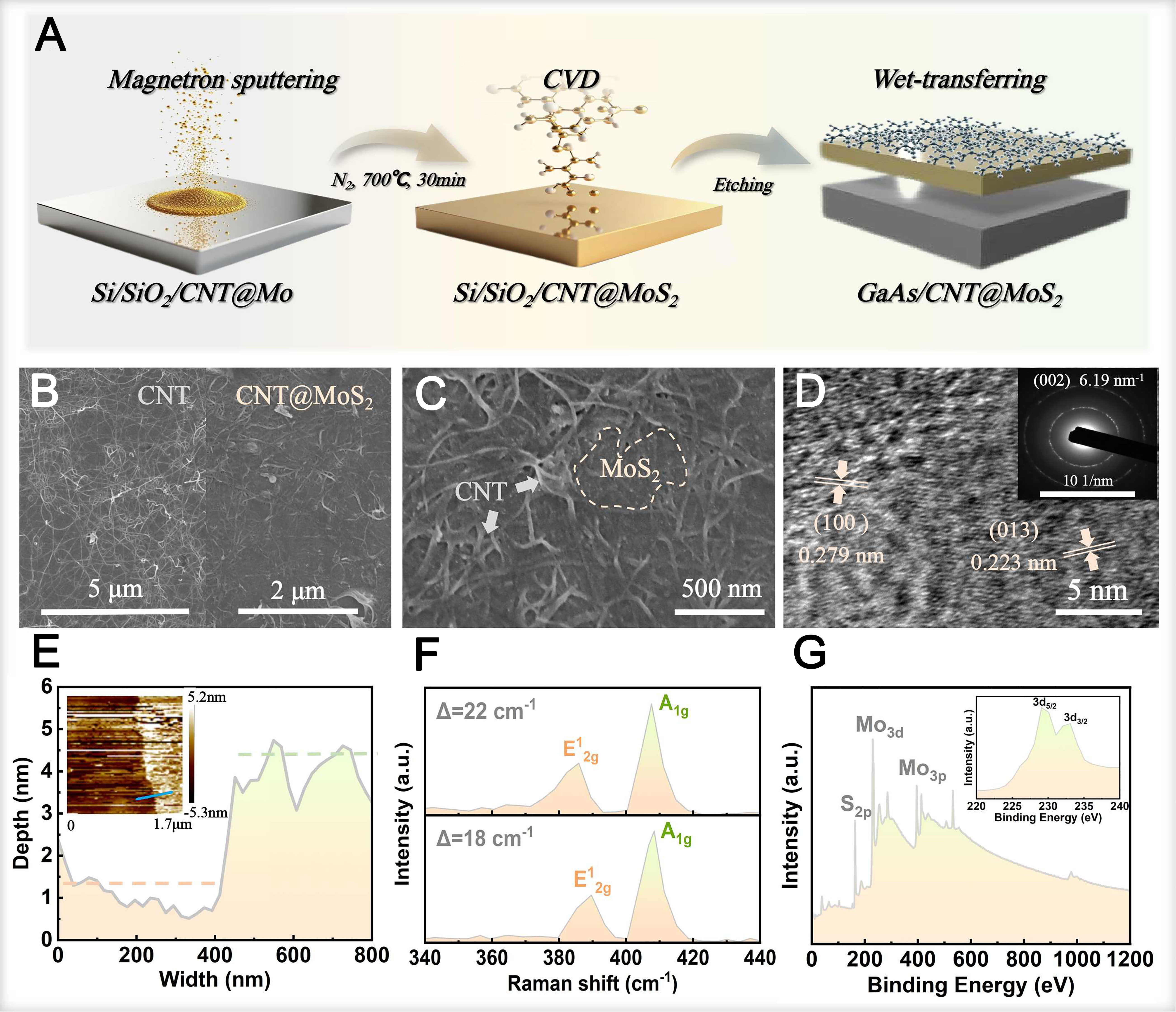
Figure 1. (A) Schematic of GaAs/CNT@MoS2 heterojunction; SEM images of (B) CNT film and (C) CNT@MoS2 film; (D) TEM images, (E) AFM images, (F) Raman and (G) XPS curves and the Mo 3d peaks (inserted curve) of the MoS2 film. GaAs: Gallium arsenide; CNT: carbon nanotube; TEM: transmission electron microscope; XPS: X-ray photoelectron spectroscopy; CVD: chemical vapor deposition; SEM: scanning electron microscope; AFM: atomic force microscope.


