

fig2
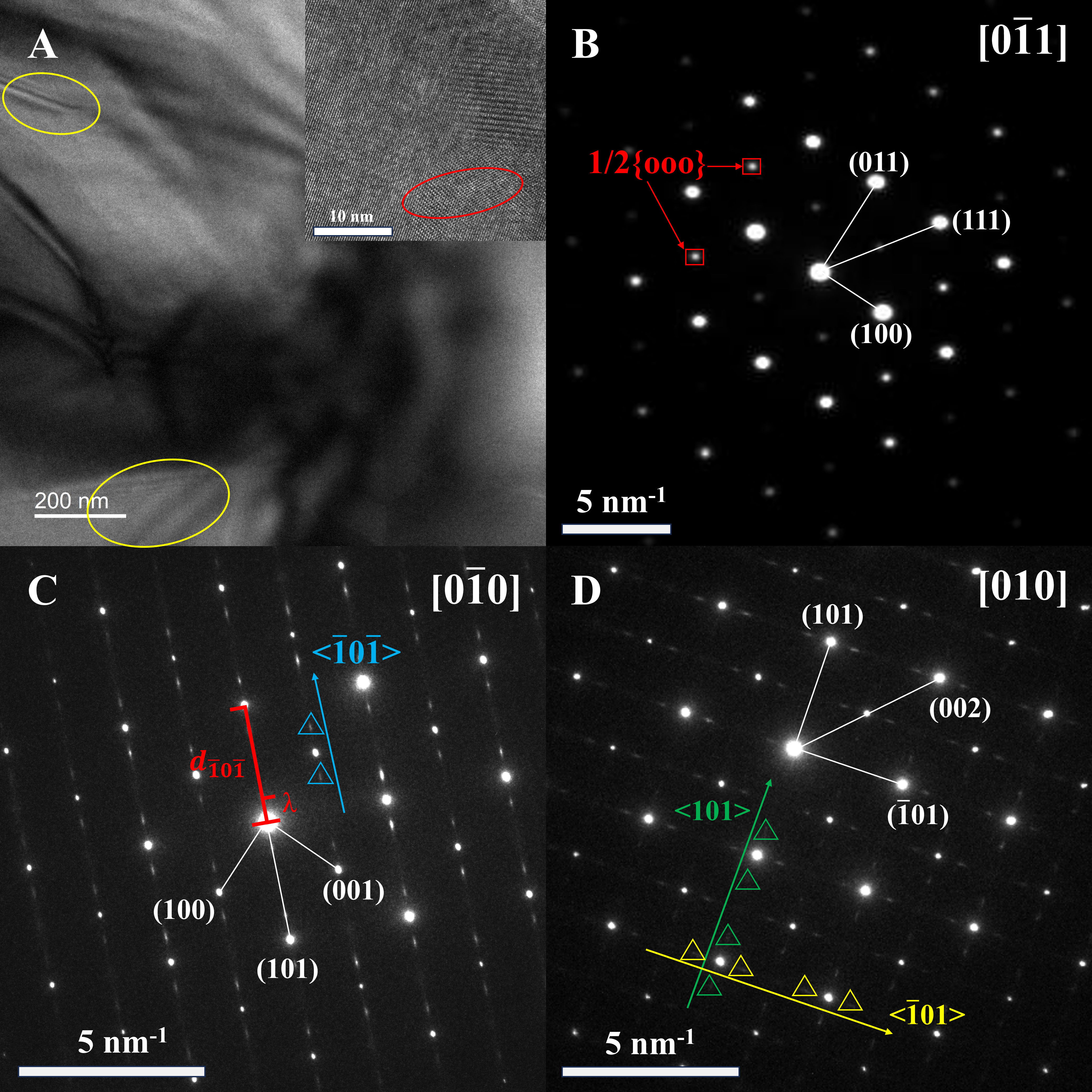
Figure 2. TEM image and diffraction patterns for PLSBZST2 (x = 0.06) AFE thick-film ceramics. (A) Bright-field images of the stripe domains, and the inset shows an HRTEM image of a nanosized domain; (B) SAED pattern with 1/2{ooo} superlattice patterns (F-spots); (C) [