

fig4
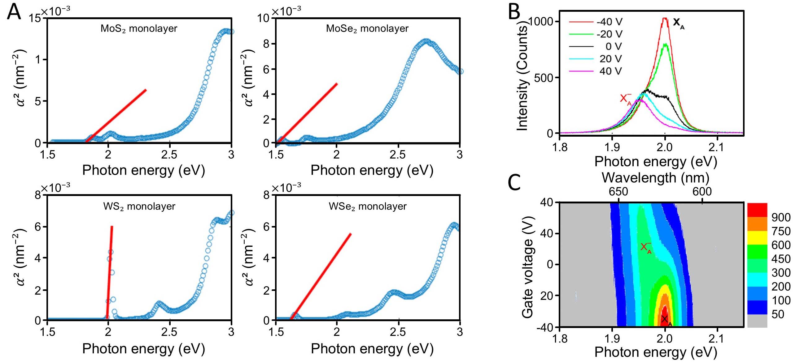
Figure 4. (A) Optical band gap graphs for monolayer TMDs (MoS2, MoSe2, WS2, and WSe2), adapted with permission[70]. Copyright 2017, Licensed under CC BY 4.0; (B) photoluminescence spectra of WS2 at back gate voltages between -40 and +40 V and (C) mapping of photoluminescence intensity as a function of photon energy and gate voltage. (B and C) are adapted with permission[74]. Copyright 2015, American Chemical Society.