

fig3
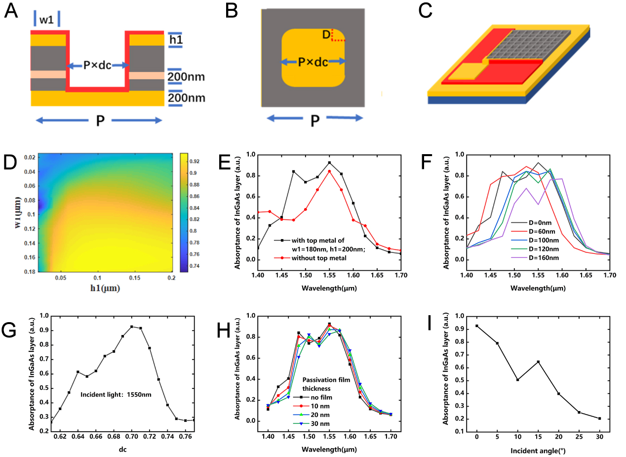
Figure 3. (A) x-z cross-section of the grid UTC-PD unit with SiO2 passivation films. The gray part includes layers 1-6 in Table 1 with a total thickness of 850 nm, and the thickness of the lower electrode is set to 200 nm; (B) x-y cross-section of the grid UTC-PD unit. D is the radius of the arc at the grid corner; (C) Schematic of the grid UTC-PD device with the top electrode prepared only at the edge of the upper layer; (D) Width (w1) and height (h1) of the top metal versus AInGaAs,x of grid UTC-PD under 1,550 nm x-polarized light illumination; (E) AInGaAs,x spectra of the grid UTC-PD with the ideal top metal morphology (black line, w1 = 180 nm, and h1 = 200 nm) and without the top metal (red line, w1 = 0 nm, and h1 = 0 nm); (F) AInGaAs,x spectra of the grid UTC-PD for different radii of the arcs at grid corners (D); (G) Air duty cycle (dc) versus AInGaAs,x of the grid UTC-PD under 1,550 nm x-polarized light illumination; (H) AInGaAs,x spectra of the grid UTC-PD for different passivation film thicknesses; (I) AInGaAs,x of the grid UTC-PD at 1,550 nm under x-polarized light versus the incident angle. UTC-PD: Uni-traveling-carrier photodiode.