

fig2
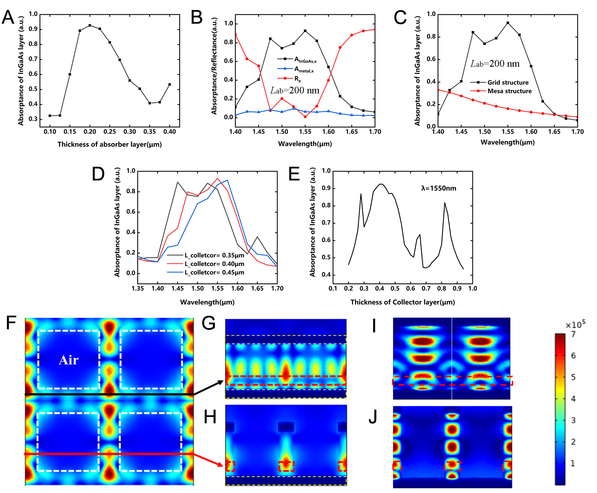
Figure 2. (A) Absorber layer thickness versus the absorption efficiency of the absorber layer 2 (AInGaAs,x); (B) Absorptance and reflectance spectra of the grid UTC-PD with Lab = 200 nm. AInGaAs,x denotes the absorption efficiency of the absorber layer-2, Ametal,x denotes the absorption efficiency of the metal, and Rx denotes the reflectance of x-polarized light; (C) AInGaAs,x of the grid UTC-PD and mesa UTC-PD; (D) AInGaAs,x spectra for different thicknesses of collector layer 5 (Lcollector); (E) Thickness of layer 5 versus AInGaAs,x; (F) Field distributions in the x-y cross-section at the middle of the absorber layer of 2 × 2 grid units; Lab = 200 nm, Lcollector = 400 nm. The white dotted box outlines enclosed air; the rest of the area includes the detectors; (G and H) Field distributions in the x-z cross-section at the black line and the x-z cross-section at the red line. Inside the red dotted box is the absorber layer. Inside the yellow dotted box is the metal; (I and J) Field distributions in the x-z cross-section inside the grid device; Lab = 200 nm, Lcollector = 820 nm. Inside the red dotted box is the absorber layer. Inside the yellow dotted box is the metal. UTC-PD: Uni-traveling-carrier photodiode; Lab: thickness of the absorber layer.