

fig1
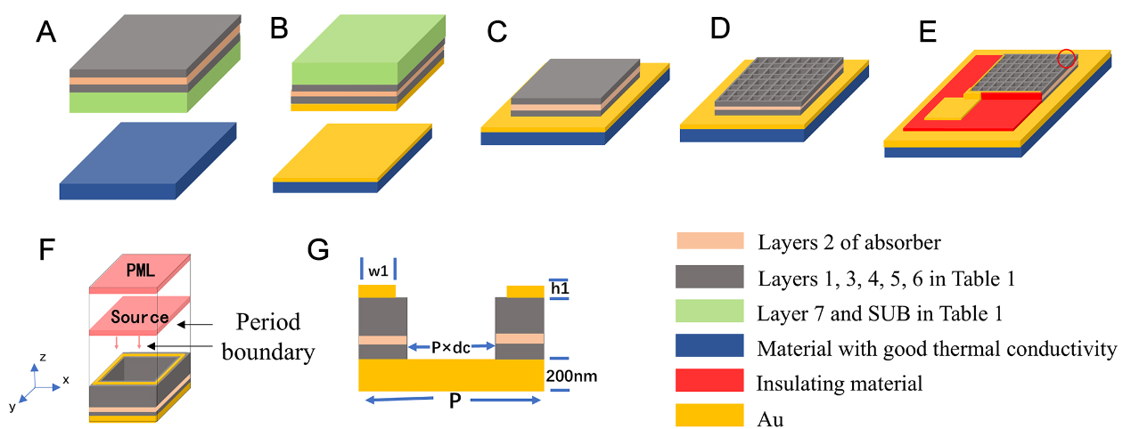
Figure 1. (A-E) Flowchart of the proposed fabrication process for the grid UTC-PD. (A) Thermally conductive material (blue) and detector epitaxial wafers (gray, pink and green); (B) growth of metal (yellow) on the thermally conductive material and epitaxial wafer; (C) metal bonding and complete substrate removal for the epitaxial wafer; (D) etching of the grid structure; (E) preparation of the upper metal electrode, with the red part denoting the insulating material; (F) Schematic of the grid UTC-PD unit; (G) x-z cross-section of the grid UTC-PD unit, the gray part includes layers 1-6 in Table 1; the thickness of the lower electrode was set to 200 nm. UTC-PD: Uni-traveling-carrier photodiode; SUB: substrate.