


fig6
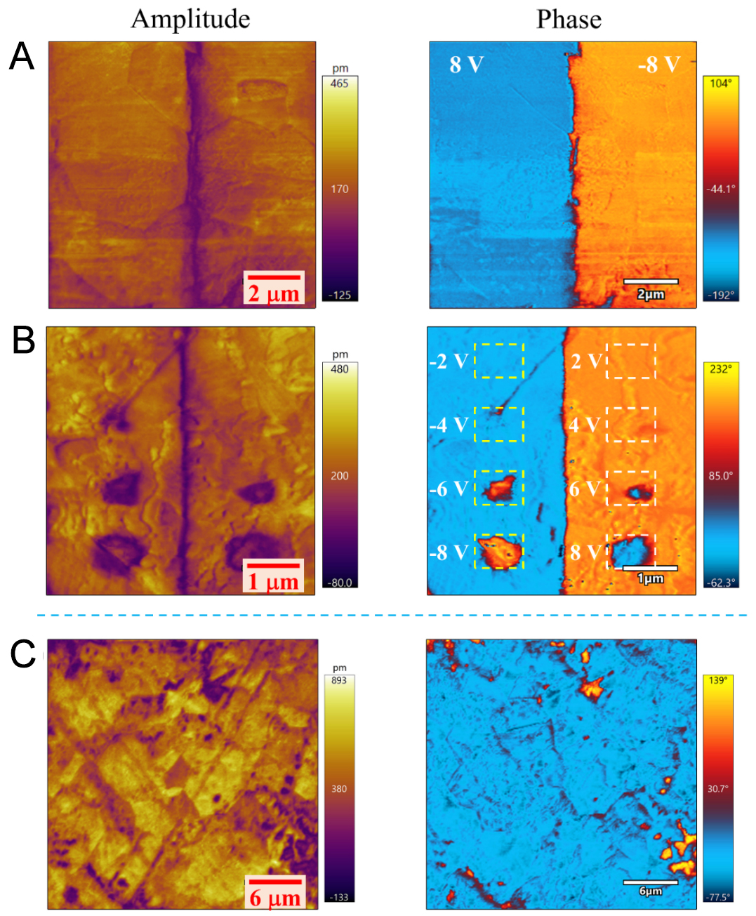
Figure 6. (A and B) PFM images of amplitude switching and phase switching under positive and negative tip DC voltages for the unpoled 0.555PNN-0.145PZ-0.30PT ceramic; (C) PFM images of the 15 kV/cm DC electric field-poled 0.555PNN-0.145PZ-0.30PT ceramic. The domain structure areas in (A), (B), and (C) are 10 μm × 10 μm, 5 μm × 5 μm, and 30 μm × 30 μm, respectively. DC: Direct current; PFM: piezoelectric force microscopy.


