fig17

Multiscale microstructure design for high-performance dielectric energy storage materials

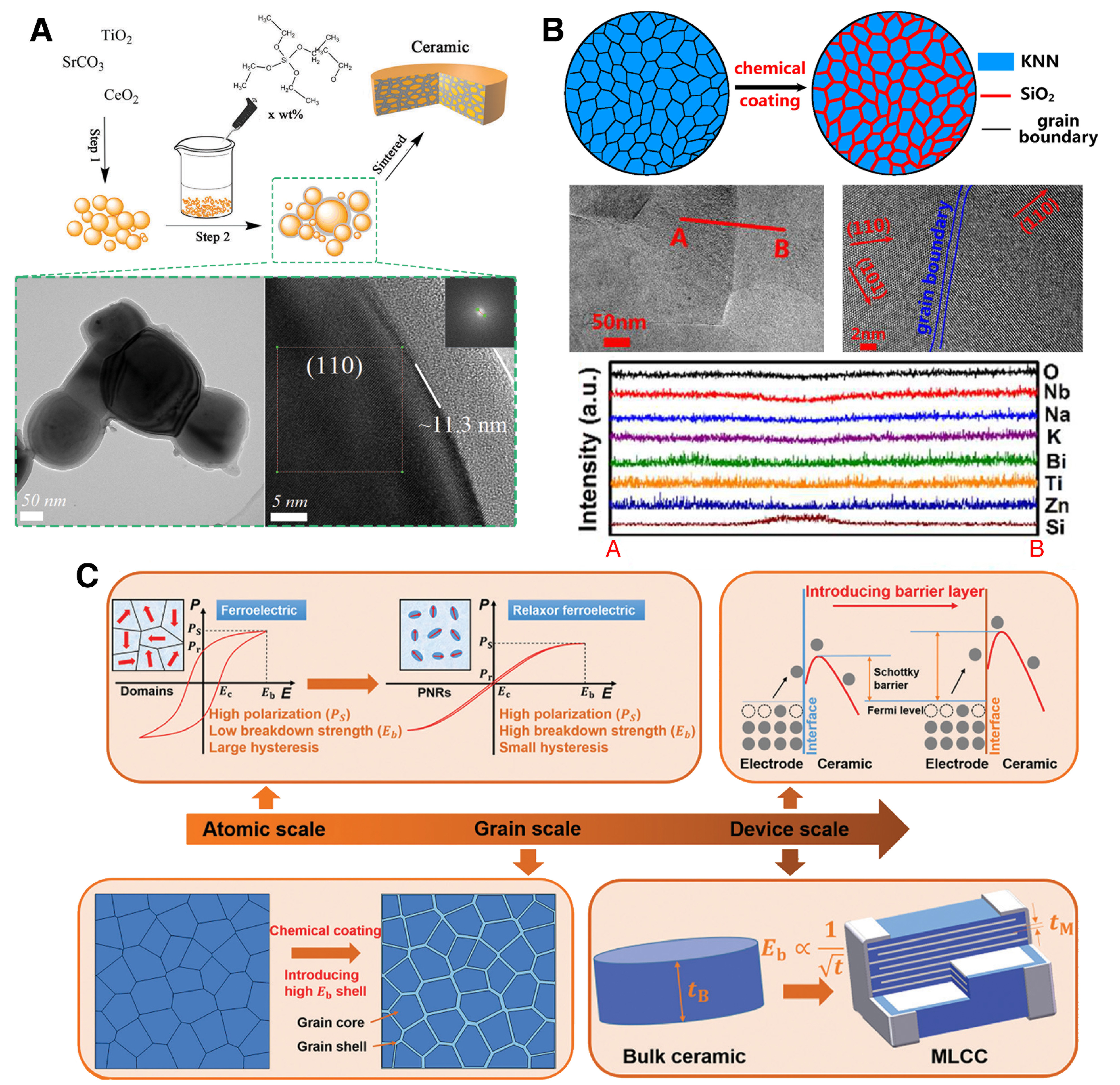
Figure 17. Grain boundary engineering enhances BDS to optimize ESP. (A) Experimental processing route and field-emission TEM images of [email protected] wt% SiO2; inset shows FFT of the selected area. Step 1: Ce-doped SrTiO3 powders synthesized via the solid-state method. Step 2: Pre-doped powders coated with varying amounts of tetraethoxysilane (TEOS) using the Stöber process. This figure is quoted with permission from Qi et al.[144]; (B) Schematic of grain configurations in KNN and KNN@SiO2 FE ceramics, alongside microstructure topography and elemental distributions of KNN-BZT@SiO2 ceramics. This figure is quoted with permission from Huan et al.[71]; (C) Schematic illustrating multiscale optimization strategies to achieve ultrahigh ESP in lead-free MLCC based on RFE 0.87BT-0.13Bi(Zn2/3(Nb0.85Ta0.15)1/3O3@SiO2 MLCCs. This figure is quoted with permission from Zhao et al.[149]. BDS: Dielectric breakdown strength; ESP: energy storage performance; TEM: transmission electron microscopy; KNN: (K0.5Na0.5)NbO3; FE: ferroelectric; MLCCs: multilayer ceramic capacitors; BZT: Ba(Zr0.4Ti0.6)O3; RFE: relaxor ferroelectric; FFT: fast Fourier transform.

Microstructures
ISSN 2770-2995 (Online)

Portico

All published articles are preserved here permanently:

https://www.portico.org/publishers/oae/

Portico

All published articles are preserved here permanently:

https://www.portico.org/publishers/oae/