


fig11
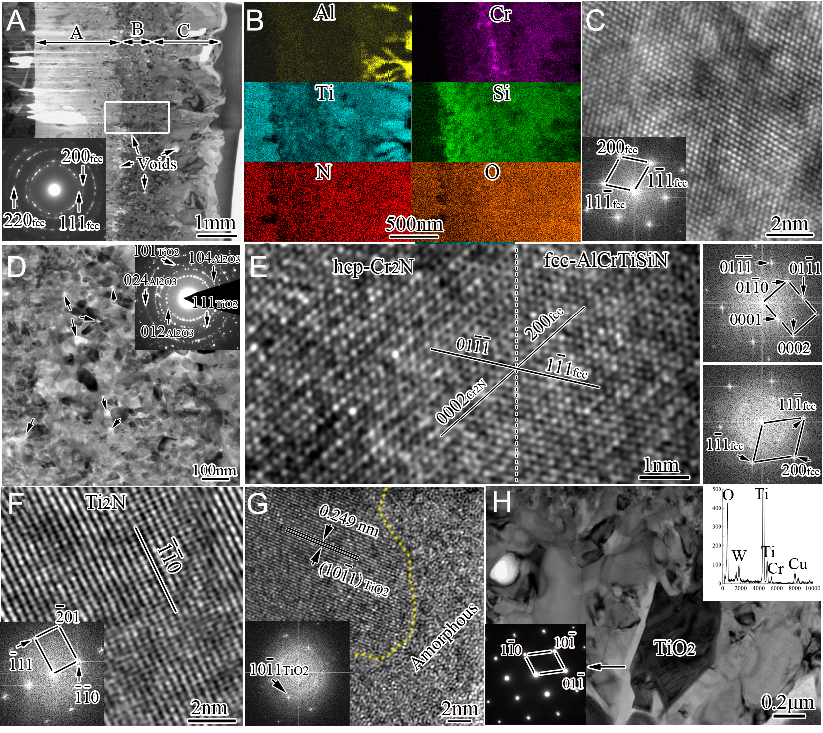
Figure 11. (A) Cross-sectional TEM image of sample No. 9 oxidized at 1,000 °C, with the inset showing the SAEDP obtained from region “A”; (B) EDS mapping of Al, Cr, Ti, Si, N, and O in the region outlined in (A); (C) HRTEM image of a representative zone within the “A” sublayer; (D) High-magnification TEM image of a region in the “B” sublayer; (E) HRTEM image of a Cr-rich domain at the “A/B” interface, with the corresponding FFT pattern shown in the inset; (F-G) HRTEM images of Cr2N, fcc-AlCrTiSiN, Ti2N, and TiO2 grains within the “B” sublayer; (H) TEM image of coarse TiO2 grains, with indexed SAEDP and EDS point analysis shown in the insets.


