

fig3
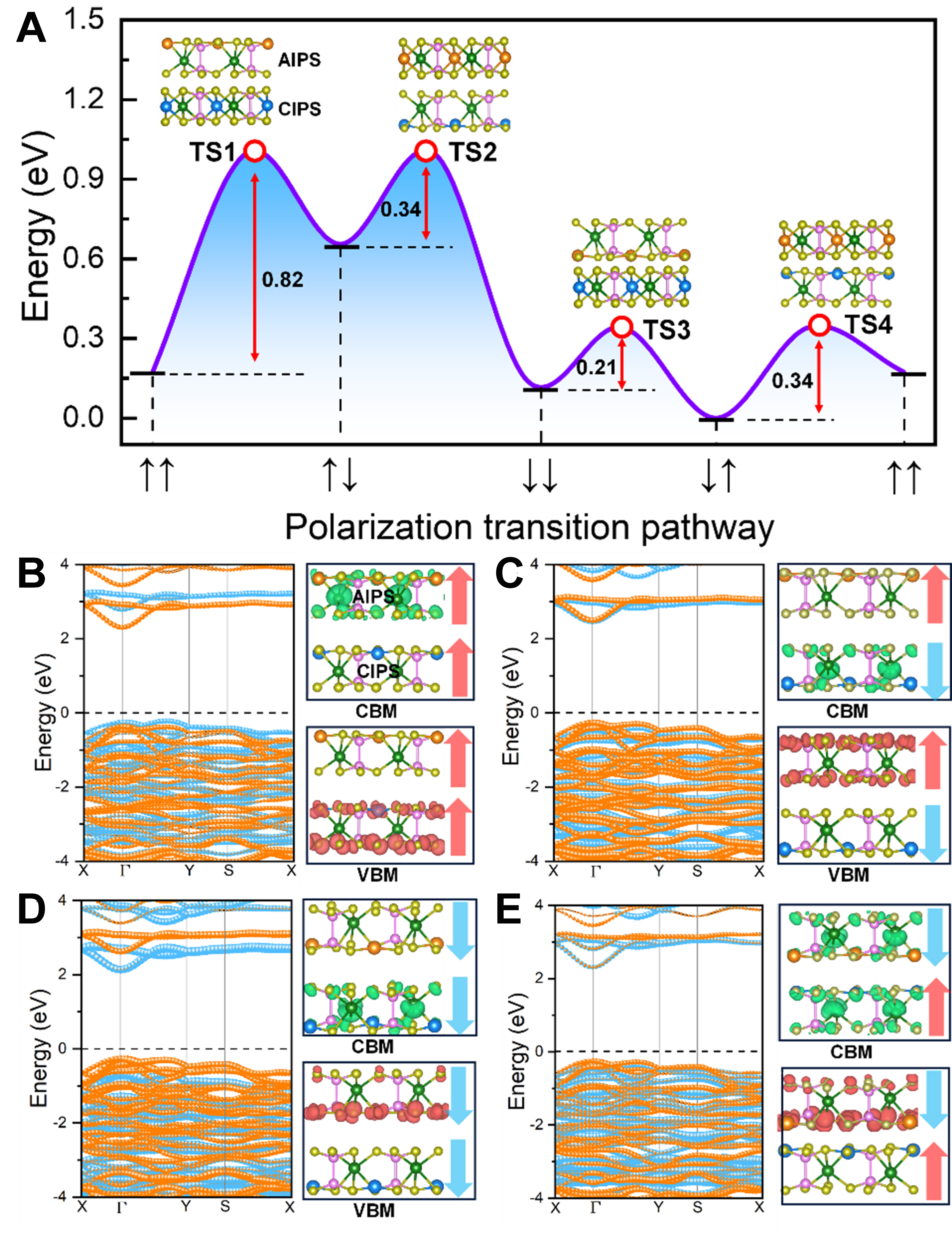
Figure 3. Polarization switching energy profile and electronic properties of 2D CIPS/AIPS VFSH in four polarization states. (A) Energy profile of FE switching among four polarization states in 2D CIPS/AIPS VFSH. TS1-TS4 denote the transition states from one polarization state to another, and the numbers correspond to the energy barriers for activating the transition of polarization states; (B-E) The projected band structure (left panel) and spatial charge-density distribution (right panel) of CBM and VBM states of CIPS/AIPS VFSH in (B) ↑↑, (C) ↑↓, (D) ↓↓, and (E) ↓↑ calculated by the HSE06 functional. The horizontal dashed line in the band structures denotes the Fermi level. The yellow and blue bands are contributed by AIPS and CIPS layers in the heterojunction, respectively. 2D: Two-dimensional; CIPS/AIPS: CuInP2S6/AuInP2S6; VFSH: vdW FE semiconductor heterojunction; FE: ferroelectric; CBM: conduction band minimum; VBM: valence band maximum.