

fig1
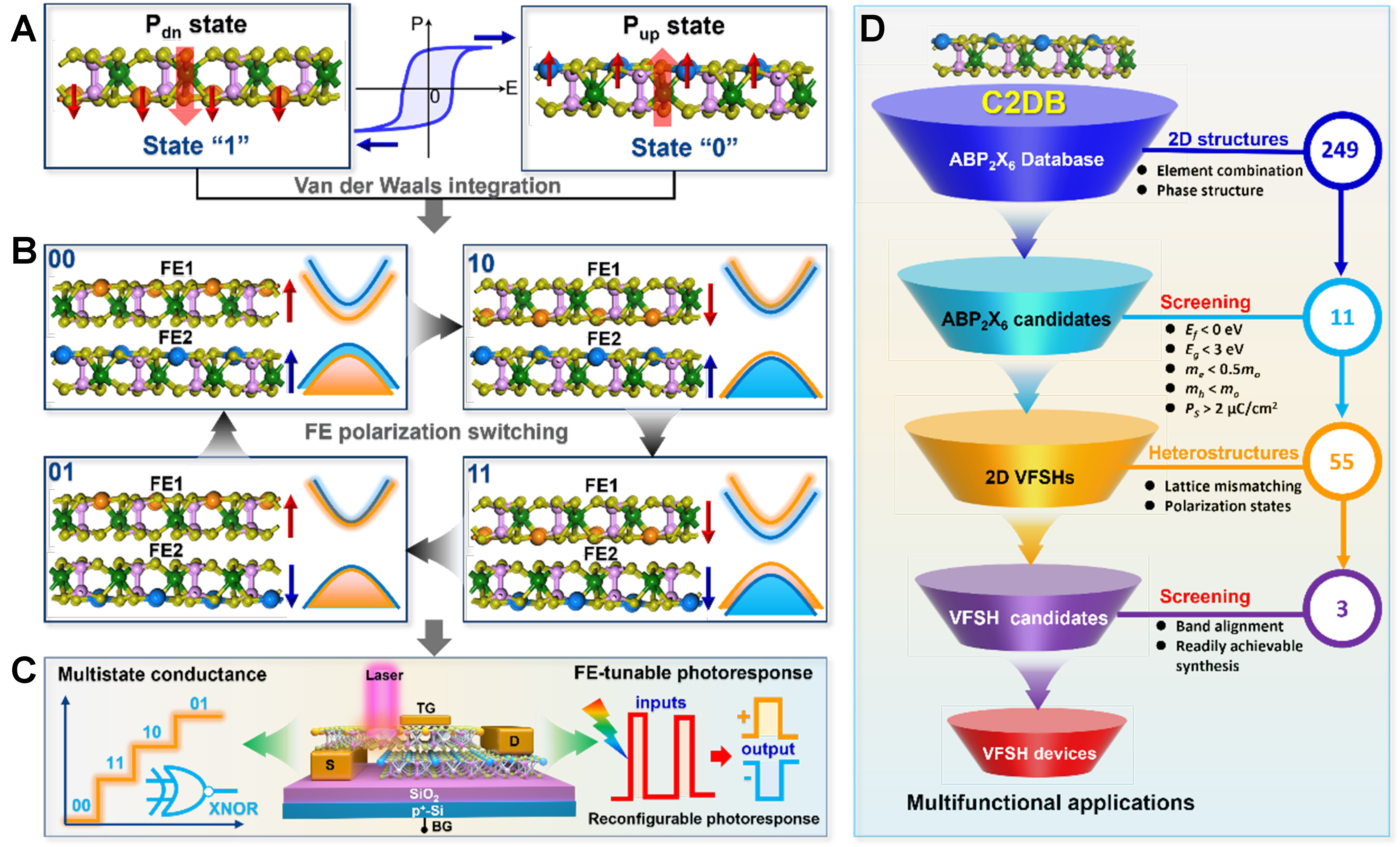
Figure 1. Basic principle and high-throughput computational screening flow of 2D ABP2X6 VFSHs for constructing all-in-one optoelectronic device architecture. (A) Atomic structure and polarization orientation of 2D ABP2X6 FE semiconductors in Pdn and Pup states; (B) FE polarization orientation and schematic band alignment of 2D ABP2X6 VFSHs in four stable polarization states (i.e., ↑↑, ↓↑, ↓↓, and ↑↓); (C) Basic concept of 2D ABP2X6 VFSH devices with FE-tunable electric and optoelectronic properties for multifunctional applications; (D) High-throughput computational screening workflow and framework of 2D ABP2X6 VFSHs for multifunctional device applications. 2D: Two-dimensional; VFSHs: vdW FE semiconductor heterojunctions; FE: ferroelectric; TG: top gate; BG: back gate; C2DB: computational 2D materials database.