


ABC2-type short-wave infrared photodetector materials discovered via high-throughput screening and machine learning
 0
0 Abstract
Rapid discovery of short-wave infrared (SWIR) detection materials requires efficient strategies to identify candidates with suitable bandgaps, favorable carrier transport properties, and structural stability. Here, we propose a high-throughput screening (HTS) framework that integrates machine learning (ML) models with density functional theory (DFT) calculations to accelerate the prediction and validation of infrared-detection materials [see Graphical Abstract]. Using a curated dataset of 1327 I-X-VI chalcogenide compounds retrieved from the Materials Project database, we trained five regression models-random forest, gradient boosting, support vector regression, extreme gradient boosting, and decision tree-to predict electronic bandgaps with high accuracy and computational efficiency. The optimized extreme gradient boosting regression (XGBR) model delivers a test-set coefficient of determination (R2) of 0.945, a mean absolute error (MAE) of
Keywords
INTRODUCTION
Short-wave infrared (SWIR) radiation, typically spanning wavelengths from approximately 1 to 3 μm, exhibits high detection efficiency and strong environmental penetration. Unlike other infrared regions, SWIR radiation is capable of detecting not only thermal emissions and atmospheric airglow but also reflected light from surrounding objects. These characteristics make it particularly advantageous for applications such as night vision, camouflage detection, and target recognition. In recent years, SWIR technologies have extended into civilian domains, including industrial Non-Destructive Testing (NDT), bio-component identification, and even border-coastal defense monitoring. The growing demand for high-performance and cost-effective SWIR detectors has consequently driven the development of novel materials and advanced device architectures[1-5].
Conventional materials such as mercury cadmium telluride (HgCdTe) and indium gallium arsenide (InGaAs) have long been used for SWIR detection due to their excellent optoelectronic properties. However, HgCdTe involves toxic elements and complex epitaxial growth, while InGaAs is costly and limited in detection range, restricting their broader application. Two-dimensional (2D) materials like black phosphorus, transition metal dichalcogenides (TMDs), and InSe offer high mobility and broadband absorption, but their instability, low monolayer absorption, and poor scalability hinder device-level integration[6]. As a promising alternative, lead selenide (PbSe), an IV-VI semiconductor, offers a direct and narrow bandgap ideal for SWIR detection, along with relatively mature synthesis routes. In its colloidal quantum dot (CQD) form, PbSe enables solution processing, size-tunable bandgaps extending up to 3 μm, and low-cost fabrication. Although stability and surface defects remain challenges, recent advances have pushed the detectivity of PbSe QD-based devices beyond 1011 Jones and external quantum efficiency over 120%[7], making them increasingly viable for commercial SWIR applications.
The early discovery of infrared materials primarily depended on empirical approaches and labor-intensive experimental screening, which were often time-consuming and inefficient. For instance, HgCdTe, a widely used infrared detector material, was first identified in the late 1950s and subsequently optimized through iterative experimentation with techniques such as Bridgman growth, zone melting, and quench-anneal treatment[8]. Although the advent of first-principles simulations has enabled the theoretical prediction of key material properties-such as bandgap, thermal stability, and mechanical robustness-these methods remain computationally demanding, particularly when applied to large-scale screening tasks. To address these challenges, researchers have increasingly turned to more efficient strategies for materials discovery. High-throughput screening (HTS), supported by initiatives such as the Materials Genome Project and large-scale databases including the Materials Project[9,10], allows for the rapid evaluation of thousands of candidate compounds. When combined with machine learning (ML) techniques, this approach enables the prediction of critical properties-such as bandgap, thermodynamic stability, and carrier mobility-with significantly reduced computational costs. This data-driven methodology has proven effective in the discovery of functional materials for ultraviolet and mid-infrared applications, and holds substantial promise for accelerating the development of novel infrared detection materials. It thus represents a pivotal shift toward more scalable and intelligent material design.
Recent progresses in HTS computation and ML have significantly accelerated the discovery of novel materials, particularly in the field of optoelectronics and IR applications. HTS techniques enable the rapid evaluation of thousands of candidate compounds through automated workflows, facilitating efficient materials screening based on structural and electronic descriptors[11-14]. For instance, Wang et al. performed large-scale HTS first-principles calculations to screen nearly 1,000 monolayer structures, ultimately identifying 256 thermodynamically, mechanically, dynamically, and thermally stable 2D semiconductors with desirable electronic properties[14]. The resulting database, termed the Two-Dimensional Semiconductor Database (2DSdb), provides a valuable resource for further theoretical modeling and device design. ML, on the other hand, has emerged as a powerful tool for uncovering complex structure-property relationships and accelerating predictive modeling[15-19]. Sun et al. utilized ML-assisted synthesis to develop lead-free, perovskite-inspired materials with improved stability and optoelectronic performance[19]. Similarly,
As a promising material system for high-performance SWIR photodetectors, the I-X-VI chalcogenides - corresponding to the ABC2 configuration [A = alkali metals (Li, Na, K, Rb, Cs), B = all main group and transition metal elements, C = chalcogen elements (S, Se, Te)] - integrate intrinsic advantages that address core photodetection requirements: strong covalent bonding, tunable direct bandgaps (modulated via ordered-disorder transitions or structural distortion to match the SWIR range, as verified in AgBiS2[28] and CuTlSe2[29]), excellent p-type dopability, and robust mechanical/thermodynamic stability (confirmed by first-principles calculations[30]). Composed of earth-abundant, low-toxicity elements, these compounds also exhibit high carrier mobility, suppressed non-radiative recombination, and promising optoelectronic performance [e.g., External Quantum Efficiency (EQE) exceeding 13% in relevant systems[31]], while their structural flexibility and compatibility with thin-film growth further enhance practical applicability. Collectively overcoming limitations of traditional materials (fixed bandgaps, toxicity, poor stability), the integration of HTS and ML-driven selection with targeted exploration of I-X-VI (ABC2-type) chalcogenides holds great promise for the rational design of efficient, scalable, and environmentally friendly SWIR optoelectronic materials.
To efficiently explore this chemically diverse space, we developed a HTS framework that integrates ML with DFT calculations. A curated database of I-X-VI selenide compounds was constructed, and five regression models-random forest, gradient boosting, support vector regression, extreme gradient boosting, and decision tree-were trained to predict their electronic bandgaps. This data-driven approach led to the identification of five promising IR candidates: KGaSe2, KGaTe2, KInSe2, KInTe2, and CsInTe2. Among them, KGaSe2 was found to possess an optimal bandgap (~0.8 eV), favorable carrier transport properties, and excellent thermodynamic stability, as confirmed by detailed DFT analysis.
These findings demonstrate the potential of integrating ML and first-principles methods for the accelerated discovery of high-performance IR detection materials. Compared with previous work[32], this method not only improved the accuracy and comprehensiveness of candidate material screening, but also revealed the orbital essence of performance differences through electronic structure analysis, providing a generalizable example for the design of SWIR materials.
MATERIALS AND METHODS
Overview of computational methods
This study aims to rapidly predict and screen SWIR materials with excellent absorption properties by integrating ML with HTS, and ultimately validate the screening results using first-principles calculations based on DFT. The research workflow mainly consists of three steps: HTS screening, ML, and DFT validation, as shown Figure 1. First, a material dataset covering infrared absorption properties is constructed, key descriptors are extracted, and a predictive model is established using ML algorithms. The trained model is then used to predict the infrared absorption properties of a large number of as-yet unsynthesized materials. After obtaining the prediction results from the ML model, HTS is applied to filter candidate materials. The selection criteria are primarily based on predicted bandgap ranges and other physicochemical parameters to ensure that the selected materials have potential advantages for target applications. Finally, to ensure that the screened candidate materials exhibit reliable infrared absorption properties, first-principles calculations based on DFT are performed for validation.
Figure 1. Flowchart for screening promising SWIR photodetector materials via an integrated high-throughput screening, ML, and DFT approach. Starting from ternary compounds retrieved from The MP database, this workflow first implements high-throughput screening incorporating seven specific space groups. Through predefined selection criteria, the pool is refined to yield infrared detection material candidates and corresponding initial feature parameters. The resulting dataset is then processed via ML for feature optimization to identify key representative features, followed by ML-driven material prediction to obtain potential infrared detection candidates. Finally, comprehensive DFT calculations - including bandgap computation, structural optimization, formation energy analysis, optical absorption, mechanical properties, effective mass, and DOS calculations - are performed to complete the final screening and identify the most promising SWIR photodetector materials. SWIR: Short-wave infrared; ML: machine learning; DFT: density functional theory; MP: Materials Project; DOS: density of states.
HTS framework
To identify high-performance SWIR photodetector materials, a multi-step HTS framework was developed. Starting from ~30,000 ternary compounds retrieved from the Materials Project database, sequential filters were applied based on symmetry, composition, stoichiometry (ABC2-type[33,34]) and atomic complexity, reducing the pool to 1327 non-toxic, structurally feasible candidates. The initial band gap values used for screening were obtained directly from the Materials Project database. A ML model was then trained to predict infrared bandgaps, and 278 compounds meeting the target bandgap features were obtained, including those in the SWIR range (0.41-0.89 eV)[35]. Subsequent constraints on bandgap, mechanical and dynamical stability, as well as optical and transport properties, led to a final shortlist of robust candidates with strong potential for SWIR optoelectronic applications.
ML methods
In this study, we integrated ML with DFT calculations to screen potential three-dimensional (3D) materials for SWIR photodetector and structural stability, targeting bandgap width as the key predictive property for ML modeling. Based on elemental composition and spatial configurations, through preliminary screening and literature research, a ML database consisting of 1327 materials and 220 initial characteristic variables was finally constructed. Five ML algorithms-Random Forest Regression (RFR), Gradient Boosting Regression (GBR) and Support Vector Regression (SVR), extreme gradient boosting regression (XGBR), and Decision Tree (DT)[36,37] were implemented using the Scikit-Learn library and compiled via Jupyter Notebook[38,39]. The dataset was randomly partitioned into an 80% training set and a 20% testing set for model training and performance validation.
DFT calculations
Density functional theory (DFT) calculations were performed using the Vienna Ab initio Simulation Package (VASP) based on the projector augmented wave (PAW) method. The process also made use of plane-wave pseudo potentials[40,41]. To represent electron wave functions, a plane-wave basis set with a uniform kinetic energy cutoff energy of 500 eV for all calculations. The exchange-correlation interactions were treated within the generalized gradient approximation (GGA) using the Perdew-Burke-Ernzerhof (PBE) functional. Structural optimizations were carried out until the total energy convergence reached 10-5 eV, and the residual Hellmann-Feynman forces on each atom were smaller than 0.01 eV·Å-1. To accurately characterize the band structure features of the material, k-point sampling is carried out along the high-symmetry points of the Brillouin zone during the calculation process, in order to reveal the distribution laws of electronic states in different momentum space regions[42].
To maintain consistent computational accuracy across diverse crystal systems, Γ-centered k-point meshes were chosen to deliver comparable resolution in reciprocal space. The convergence of key properties with respect to k-point density - along with the associated k-point spacings for representative structures - is documented in the Supplementary Materials. Specific mesh dimensions were tailored according to each system’s symmetry and lattice parameters, exemplified by a 4 × 4 × 2 mesh for space group I41/amd, 3 × 3 × 3 for I4̅2d, and 9 × 9 × 1 for R3̅m. The high-symmetry locations for the band structures were found to be, respectively, G (0 0 0), F (0 0.5 0), Q (0 0.5 0.5), Z (0 0 0.5) and G (0 0 0). K-point convergence tests were performed for representative I41/amd and R3̅m structures. Total energy, band gap convergence, and estimated k-point spacings are summarized in Supplementary Tables 1 and 2 of the Supporting Information. And the crystal structures were displayed using Visualization for Electronic and Structural Analysis (VESTA). The crystal structures were displayed using VESTA.
RESULTS AND DISCUSSION
High-throughput calculation
We start with all possible ternary chalcogenide structures from the Materials Project database[43]. Considering the difficulties in synthesizing multicomponent materials, we focus on ternary compounds, which account for approximately 30,000 materials. Further, we introduce a series of screening criteria in order to identify the most promising material candidates for SWIR photodetector potential candidates. And the candidate space groups include 7 types, namely C2/c, I4̅2d, I4/mcm, R3̅m, Pna21, I41/amd, and P4/mmm. The selection of these seven space groups is not arbitrary but based on their statistical prevalence in stable ABC2-type (I-X-VI) chalcogenides, structural compatibility with SWIR photodetection performance, and verified synthetic feasibility[44-46]. Our screening workflow is schematically presented in Figure 2A and illustrated as follows.
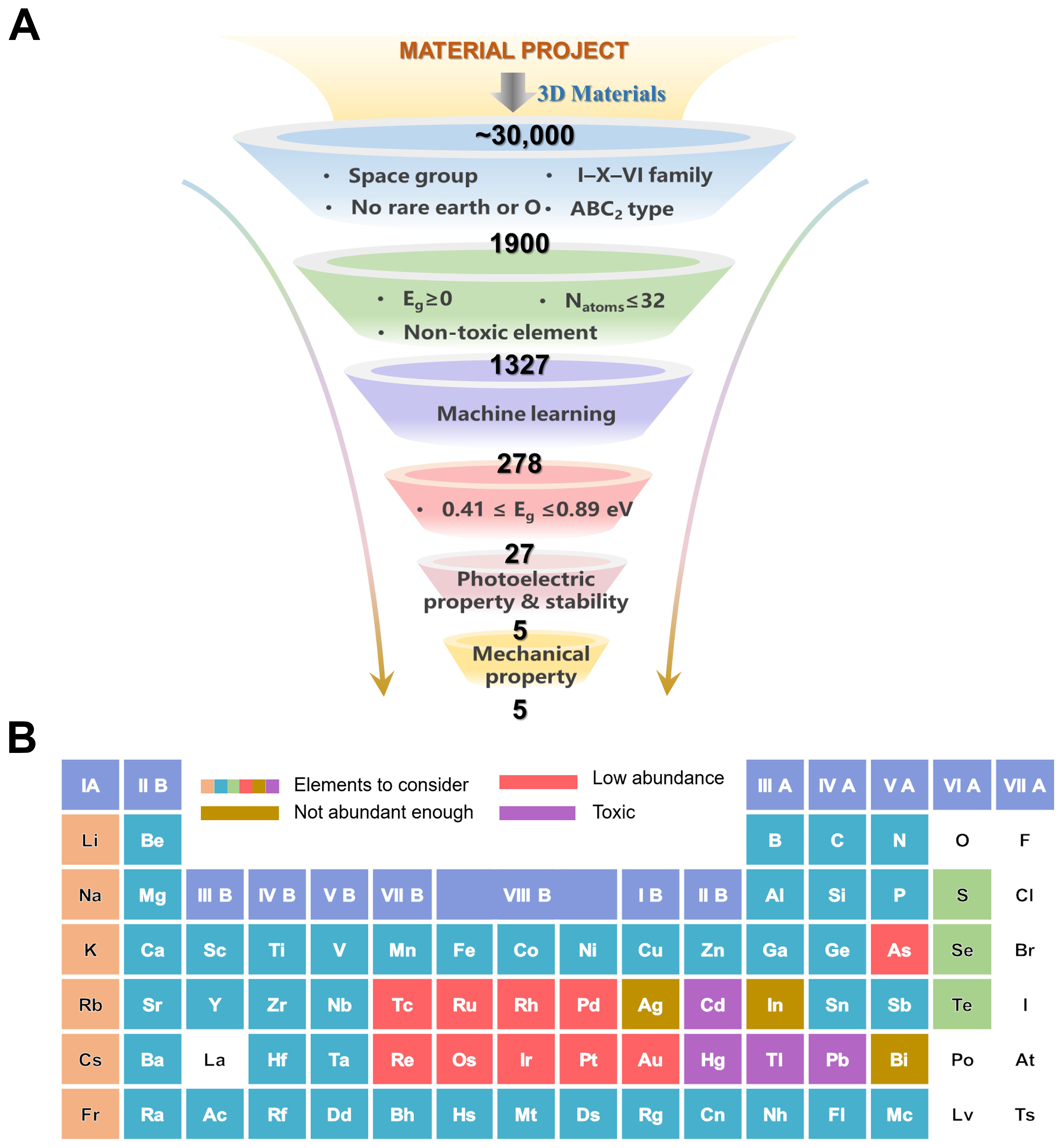
Figure 2. (A) HTS workflow for the computational screening of promising infrared detection materials; (B) The database of candidate materials, with the constituent elements shown in the figure. HTS: High-throughput screening.
Among them, C2/c belongs to the monoclinic crystal system and is a stable structure that can adapt to distortion effects. Materials with this structure have good structural stability under external field effects. I4̅2d, I4/mcm and I41/amd all belong to the tetragonal crystal system. I4̅2d has non-centrosymmetric characteristics and is suitable for infrared detection. I4/mcm has rotational symmetry and translational symmetry and is suitable for optoelectronic materials. I41/amd originates from the rock salt structure’s six-coordination structure and has potential application value in narrow bandgap semiconductor research. R3̅m belongs to the trigonal crystal system and is also a six-coordination structure derived from the rock salt structure. Its high symmetry helps stabilize the electronic structure of the material and improve the carrier transport capability, making it important in infrared detection materials. Pna21 belongs to the orthorhombic crystal system and is commonly found in polar materials, with wide applications in optoelectronic functional materials. P4/mmm, as the most symmetrical structure in the tetragonal crystal system, its high symmetry contributes to the isotropic optoelectronic properties of the material - which is beneficial for large-area, uniform SWIR detector fabrication.
It is important to clarify that excluding other space groups does not mean they are inherently unstable or unable to adapt to distortion, but rather they fail to meet the comprehensive requirements of SWIR photodetectors (synergy of bandgap matching, high carrier mobility, and synthetic feasibility). For example, some high-symmetry space groups (e.g., Fm-3m) are stable but have fixed bandgaps outside the SWIR range, while low-symmetry ones (e.g., P1) suffer from insufficient carrier mobility. Thus, the seven selected space groups represent a rational trade-off for target applications.
As shown Figure 2A, we introduced a series of screening criteria to identify promising SWIR detection materials. The overall screening workflow is presented as following:
Step 1: Starting from ~30,000 ternary compounds in the Materials Project database, we applied initial filters to narrow down candidates: (i) inclusion in one of 7 representative space groups; (ii) I-X-VI family; (iii) no rare earth or O and (iv) ABC2-type stoichiometry constraint. These criteria reduced the dataset to 1,900 compounds.
Step 2: To further narrow down the candidates, compounds with a non-zero bandgap (Eg > 0 eV) as reported in the Materials Project database, a total number of atoms per unit cell ≤ 32, and composed only of non-toxic elements were selected. This refinement yielded 1,327 compounds.
Step 3: A ML model was trained using 1,327 high-throughput-screened ABC2-type compounds as the training dataset to learn structure-infrared bandgap relationships. Based on the trained model and literature-guided targeted element substitutions[44-46], a prediction space was constructed for bandgap inference of unexplored ternary compounds. The trained model was then applied to this space, yielding 278 predicted sets that meet the bandgap requirements for functional infrared materials.
Step 4: In this section, a bandgap filter in the range of 0.41-0.89 eV, corresponding to the SWIR region, was imposed. These combined criteria reduced the candidate list to 27 compounds.
Step 5: Optical screening was performed by analyzing the absorption spectra. Materials that exhibited absorption coefficients below 104 cm-1 in the SWIR range were excluded. This filtering step reduced the candidate list to 5 candidates with strong SWIR optical absorption.
Step 6: The remaining 5 compounds were subjected to comprehensive first-principles calculations to evaluate their mechanical properties and dynamical stability. Elastic constants (Cij) were computed to assess mechanical robustness, and Ab initio molecular dynamics (AIMD) simulations were conducted to verify thermal stability at finite temperature. All 5 materials were confirmed to be stable under both criteria.
ML screening
Based on the chemical composition and structural characteristics of ternary compound, a ML database was constructed using elements from group. As shown Figure 2B, the first-site elements were selected from group I elements (Li, Na, K, Rb, Cs) and the last-site elements from group VI elements (S, Se, Te). This selection resulted in a dataset comprising 1,327 compounds, sourced from the Materials Project. The bandgap distribution of these 1,327 ternary compounds spans a range from 0 to 7 eV, encompassing the primary bandgap range relevant for IR optoelectronic detection materials, as illustrated in Figure 3A. For the development and evaluation of the ML model, 1,061 materials were selected as the training set, and 266 materials were chosen as the test set. The selection of feature variables for different ML prediction tasks varies; ideal feature variables can significantly enhance the predictive ability and generalization capability of the ML model. Therefore, the selected feature variables should be as rich as possible to effectively define the physical and chemical properties of the materials.
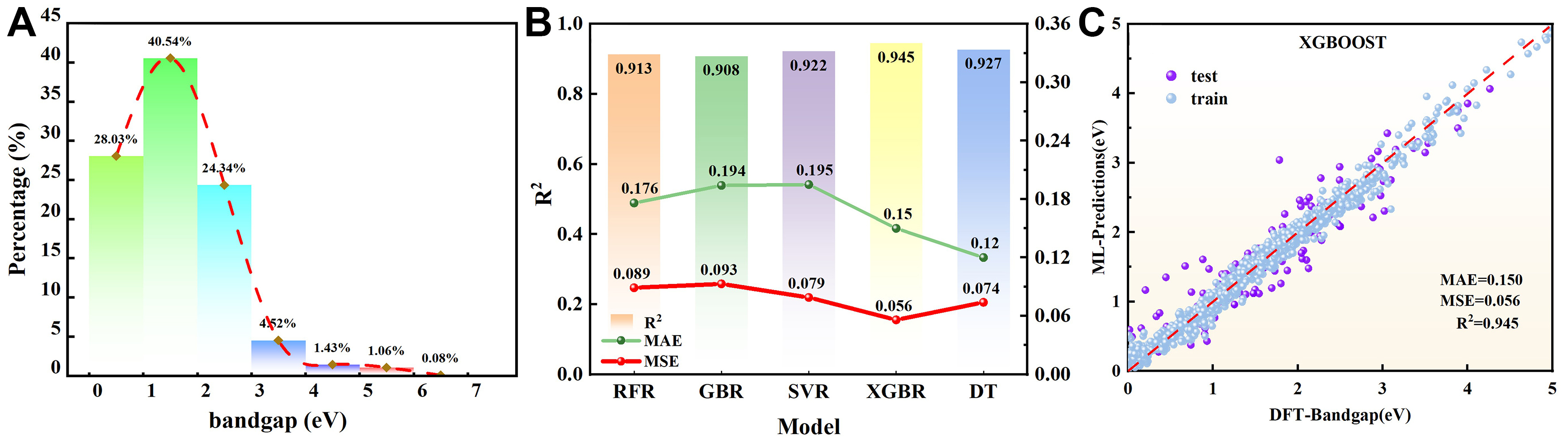
Figure 3. ML model training and prediction results. (A) The bandgap distribution of the 1,327 materials; (B) Test set performance (R2, MAE, MSE) for the five base ML models; (C) Fitting plot of the training and test set. prediction results for the best model, XGBR. ML: Machine learning; R2: coefficient of determination; MAE: mean absolute error; MSE: mean squared error; XGBR: extreme gradient boosting regressor.
When selecting feature variables, two fundamental principles should be followed: features must be easy to obtain, and the selected features must be sufficiently comprehensive and complete. The number of feature descriptors should be significantly smaller than the number of materials in the database, as too many features can reduce the predictive power and accuracy of ML models. To enable the ML model to better capture the relationship between feature variables and bandgaps, this study selected over 30 core initial features for model training, which included ion radius, valence electron count, tolerance factor, electronegativity, Fermi level, etc. However, excessive features can lead to data redundancy, thereby affecting the model’s accuracy and training speed. On the other hand, too few features may cause underfitting, preventing the model from identifying the correlation between features and bandgaps. Therefore, this study used Pearson correlation coefficient plots and importance rankings from the best training model XGBR for feature selection. Researchers first evaluated features with a Pearson correlation coefficient less than 0.7 using the correlation matrix [Supplementary Figure 1]: for each pair of highly correlated features, one was removed. Then, based on feature importance ranking, the top 21 features were selected, including the bandgap of ternary compounds, the electron affinity of elements, the Fermi level, the Mendeleev number of B-site elements, and the solid-phase average density, among others. These 21 feature descriptors are detailed in Supplementary Table 3.
We utilized five base models: RFR, SVR, GBR, DT, and XGBR. These five ML models were trained and tested using the established database of 1,327 materials. Additionally, hyperparameter optimization was performed using the grid search algorithm. By splitting the dataset into multiple training and validation sets, we reduced errors caused by randomness, ensuring the stability of the model across different data subsets.
The XGBR model demonstrated superior training performance compared to five other models based on the evaluation metrics of R2, mean absolute error (MAE), and mean squared error (MSE). On the test set, it achieved an R2 of 0.945, MAE of 0.150, and MSE of 0.056, as shown in Figure 3B.
As illustrated in Figure 3C, the predicted bandgap values (0-5 eV) of the XGBR model exhibited a high degree of consistency with the actual values across both training and test sets, confirming its robust generalization capability. The generalization ability of the hyperparameters was evaluated using K-fold cross-validation. Supplementary Table 4 summarizes the hyperparameter configurations of the five base models, with the optimized hyperparameters of the XGBR model presented immediately below the table. And Supplementary Table 5 provides the band gaps and formation energies of the 27 candidate materials, where the formation energies were calculated based on total energies of fully optimized structures relative to their elemental reference phases (see Supplementary Materials for computational details), thereby supporting feasibility evaluation and experimental selection.
The optimal XGBR model was trained using 1,327 high-quality ABC2-type compounds (refined via HTS) as the training set, whose training performance is illustrated in Figure 3C, while the training outcomes of the other four supplementary models are presented in Supplementary Figure 2 for comprehensive validation of model reliability. To expand the candidate pool for SWIR photodetection, we constructed a prediction database based on well-established infrared detection materials reported in existing literature - such as the ABC2-type AgBiS2, a typical high-performance near-infrared detection material with tailored structural and electronic properties[47-51]. Specifically, we performed targeted element substitutions on the A, B, and C sites of these literature-validated materials, including substitutions of elements from the same group, as well as constrained substitutions within the same period only when the substituted elements exhibit effectively identical valence-electron configurations in the relevant bonding environment. In addition, substitutions were limited to elements with similar electronic orbital characteristics, defined here as having the same dominant valence-orbital types with effectively identical electronic configurations near the band edges without introducing additional strongly correlated d or f states. This strategy has been proven effective for tuning bandgaps within the SWIR range while retaining core material stability. These rational substitutions ensured the derived compounds retained core electronic properties consistent with the 1,327 high-quality training samples, thus maintaining structural and chemical compatibility with the ABC2-type system[52,53]. Subsequently, we applied the trained XGBR model to predict the bandgaps of compounds in this constructed database, and guided by the fundamental screening criteria for SWIR detection materials[54], 278 promising candidates were identified from the prediction results. All predicted band gaps are based on the PBE benchmark, and the actual values may be systematically higher by 30%-50%. To ensure the generalizability of our ML model for ABC2-type ternary compounds, we employed k-fold cross-validation to select the best XGBoost configuration [Supplementary Figure 3]. We compare the predicted bandgaps against the true values, with 95% confidence intervals (CI) included, in Supplementary Figure 4, and summarize the 95%CI for quantifying bandgap prediction uncertainty separately in Supplementary Table 6.
After ML identified 278 promising candidates for SWIR applications, we further refined the candidate set based on their predicted bandgap values. Specifically, compounds with bandgaps falling within the SWIR range of 0.41-0.89 eV were selected, in accordance with the fundamental bandgap requirements for SWIR photodetector materials. Based on this bandgap criterion, 27 compounds were retained from the initial 278 candidates. This selection ensures that the final candidates exhibit bandgaps well suited for SWIR detection and therefore possess strong potential for infrared optoelectronic applications. These 27 materials were subsequently chosen for detailed first-principles DFT calculations.
Crystal stability and photoelectric performance
To further assess these 27 ABC2-type candidates, we performed formation energy calculations[54,55] based on total energies of fully optimized structures relative to their elemental reference phases, and computed their electronic band gaps using the PBE functional. Concurrently, their optical absorption spectra were evaluated to determine suitability for infrared applications. This screening identified five compounds exhibiting strong absorption within the SWIR spectral range, as illustrated in Figure 4. These materials exhibit a favorable combination of low formation energies and infrared-relevant optical responses, highlighting them as promising candidates for further exploration toward SWIR photodetector-related applications.
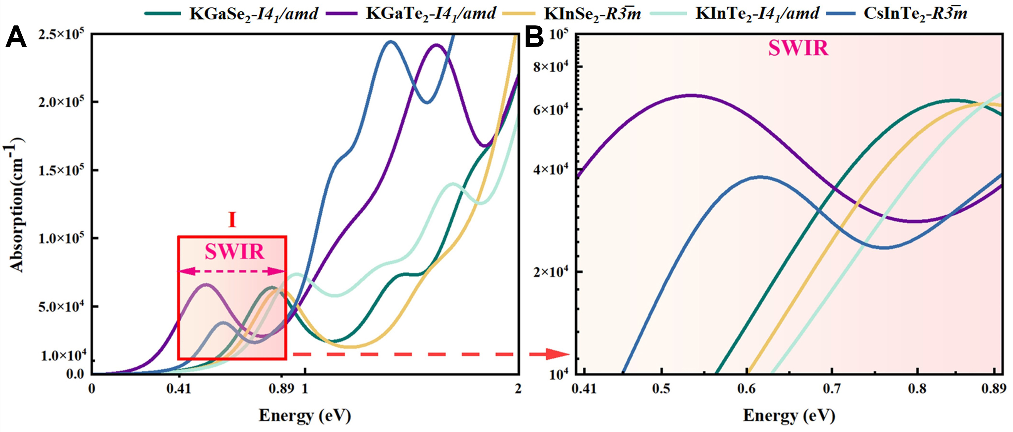
Figure 4. (A) Absorption for the five materials KGaSe2-I41/amd, KGaTe2-I41/amd, KInSe2-I41/amd,KInTe2-I41/amd, CsInTe2-R3̅m; (B) An enlarged view of Area Ⅰ in Figure 7A.
As shown Figure 4A. KGaSe2-I41/amd exhibits the most pronounced narrow-band response characteristics in SWIR region, with its main absorption peak located at 0.45 eV (2.75 μm) and an absorption coefficient reaching 1.8 × 105 cm-1, surpassing that of similar materials such as KInSe2-I41/amd (1.5 × 105 cm-1).Notably, KGaTe2-I41/amd, despite having its main absorption peak at 0.65 eV (1.91 μm), extends its absorption edge up to 1.2 eV (1.03 μm), maintaining an effective absorption coefficient of > 5 × 104 cm-1 in the SWIR-LWIR transition region. The high-symmetry I41/amd structure (e.g., KGaSe2) enhances direct bandgap transition probabilities, leading to a full width at half maximum (FWHM) of only 0.12 eV, which significantly improves spectral selectivity. Meanwhile, the layered I42d structure of CsInTe2, due to quantum confinement effects, sustains a high absorption coefficient of 1.2 × 105 cm-1 in the 1.0-1.2 eV (1.03-1.24 μm) range. This characteristic is closely associated with the strong spin-orbit coupling (SOC) effects of Te atoms. Among the five IR detection materials, the absorption spectra consistently show strong absorption edges. These properties indicate excellent optoelectronic response capabilities in IR detection materials, making these materials suitable for designing high-efficiency IR detection.
From previous literature, we know that in direct bandgap materials, the conduction band minimum (CBM) and valence band maximum (VBM) have the same momentum at the Gamma point, allowing electrons to transition directly from the CBM to the VBM without the need for lattice vibrations (phonons). The electron-hole pairs can directly recombine and emit photons[56-59]. This not only eliminates the need for complex methods such as heating, doping, quantum structure control, surface passivation, and electric field modulation, but also results in higher radiative recombination rates and photon generation efficiencies in direct bandgap materials. This characteristic significantly enhances the brightness and efficiency of devices, making candidate materials highly suitable for infrared photodetector with high recombination rates[60].
Additionally, the mechanical properties and flexibility of IR detection materials were calculated via the Young’s modulus (E). The E reflects the material’s ability to elastically deform under external force, while the shear modulus (G) characterizes the material’s resistance to shear deformation. Generally, softer materials exhibit lower E and G. Based on the calculated Cij[61], the mechanical parameters such as bulk modulus (B), G, E, and Poisson’s ratio (σ) were calculated using the Voigt-Reuss-Hill (VRH) approximation[62]. These mechanical parameters are important for evaluating the material’s mechanical stability, ductility, brittleness, and interactions, and provide a foundation for further calculations of thermodynamic parameters such as melting temperature and Debye temperature (θD). For cubic structure materials, the elastic matrix typically consists of three independent constants: C11, C12, and C44. To assess the mechanical stability of the materials, the Born mechanical stability conditions for cubic crystals at zero pressure are considered. Accordingly, the Cij (C11, C12, and C44) should satisfy the criteria C11 - C12 > 0, C11 + 2C12 > 0, and C44 > 0[63]. The quantity C12 - C44 is not a strict stability requirement but is commonly discussed as a qualitative indicator of elastic anisotropy and bonding characteristics. In addition, the condition C12 < B < C11 reflects the relationship between bulk and elastic moduli rather than serving as an independent mechanical stability criterion.
Mechanical stability is a critical parameter in evaluating the long-term reliability of SWIR detector materials. According to the Cij presented in Table 1, KGaTe2-I41/amd, and CsInTe2-R3̅m satisfy the generalized Born stability criteria, confirming their mechanical robustness.
Elastic constants and mechanical properties of KGaSe2, KGaTe2, KInSe2, KInTe2, and CsInTe2
| Compounds | C11 | C12 | C44 | C12-C44 | B | E | G | σ | B/G | θD | A |
| KGaSe2-I41/amd | 30.76 | 5.03 | 10.29 | -5.27 | 19.22 | 27.92 | 11.10 | 0.26 | 1.73 | 183.50 | 0.80 |
| KGaTe2-I41/amd | 32.75 | 6.00 | 3.75 | 2.25 | 17.57 | 19.29 | 7.32 | 0.32 | 2.40 | 132.60 | 0.28 |
| KInSe2-I41/amd | 212.93 | 12.10 | 12.42 | -0.32 | 84.95 | 80.79 | 30.11 | 0.34 | 2.82 | 271.00 | 0.12 |
| KInTe2-R3̅m | 44.09 | 20.61 | 12.90 | 7.71 | 25.22 | 32.79 | 12.77 | 0.28 | 1.97 | 165.20 | 1.10 |
| CsInTe2-R3̅m | 37.87 | 20.90 | 13.88 | 7.03 | 25.95 | 29.56 | 11.28 | 0.31 | 2.30 | 94.00 | 1.64 |
KGaTe2-I41/amd exhibits a positive C12-C44 value, indicating enhanced mechanical stability, which is commonly discussed as a qualitative indicator of elastic anisotropy and bonding characteristics rather than a strict measure of mechanical stability. This feature suggests a relatively balanced elastic response under combined normal and shear deformations, which may be favorable from a mechanical behavior perspective. CsInTe2-R3̅m, shows a higher C11, indicating a stronger resistance to uniaxial compressive deformation along the longitudinal direction. Although its relatively large C12 implies an enhanced coupling between normal stress and lateral strain, the Cij remain within a reasonable range, and its moderate C44 reflects a balanced response to shear deformation, collectively suggesting mechanically robust elastic characteristics. In contrast, KGaSe2-I41/amd and KInSe2-I41/amd both exhibit lower C44 values and negative C12-C44, which are often associated with increased elastic anisotropy and a softer shear response. These elastic features indicate a greater sensitivity to shear-related distortions and highlight potential mechanical limitations that should be considered when evaluating their structural robustness under external perturbations.
Among the studied materials, CsInTe2 shows favorable mechanical behavior in R3̅m phases. The R3̅m structure, displays higher C11 and C44 values, reflecting superior rigidity and resistance to external mechanical loads. These attributes enhance structural integrity and environmental adaptability, reducing the risk of degradation due to thermal or mechanical stress. In summary, KGaTe2-I41/amd and CsInTe2-R3̅m are mechanically stable and better suited for long-term IR detection applications. Among them, CsInTe2-R3̅m stands out for its excellent mechanical balance and should be prioritized for further development as a promising IR detector material.
Figure 5A-C present the compressive, tensile, and bending strengths of the studied materials. KGaSe2-I41/amd and KInSe2-I41/amd exhibit high bulk moduli (19.22 and 84.95 GPa, respectively), indicating strong compressive resistance suitable for long-term stable operation and physical shock absorption in optoelectronic devices.
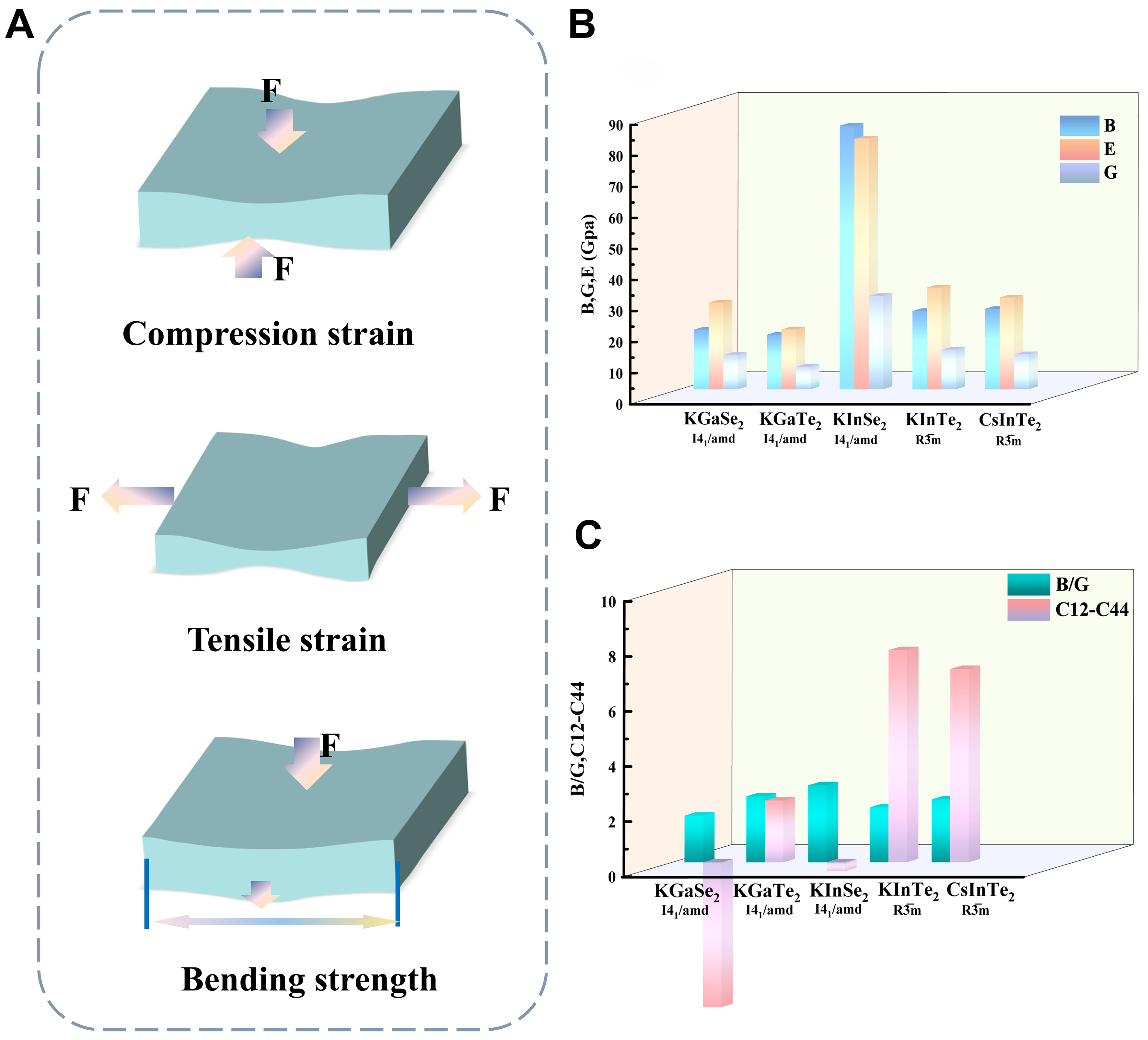
Figure 5. (A-C) Schematic diagrams of compressive strength, tensile strength, and bending strength. The elastic moduli B, G, and E are plotted in (B). (C) The Pugh’s ratio (B/G) and Cauchy pressure (C12-C44) of 5 materials. E: Young’s modulus.
The E, a measure of stiffness, is critical for assessing rigidity. KInSe2-I41/amd (80.79 GPa) and CsInTe2-R3̅m (29.56 GPa) demonstrates strong rigidity, helping maintain structural stability under mechanical and thermal stress. Similarly, the G follows the same trend: KInSe2- I41/amd (30.11 GPa) and CsInTe2-R3̅m (11.28 GPa) offers good resistance to mechanical stress. According to the Pugh ratio (B/G), which indicates ductility (with values > 1.75 denoting ductile behavior), all materials exceed this threshold. KGaTe2-I41/amd and CsInTe2-R3̅m (B/G = 2.40 and 2.99, respectively) strike a better balance between ductility and stability, making them promising for durable optoelectronic applications. The Cauchy pressure (C12-C44), an indicator of bond character and elastic behavior, is positive for all materials, implying ionic bonding and further supporting their ductile nature. σ, which measures lateral deformation, ranges between 0.32 and 0.36 for these materials. KGaTe2-I41/amd and CsInTe2-R3̅m, with slightly lower σ, offer better deformation resistance, making them more suitable for flexible detection applications. The θD, reflecting thermal stability, is highest for KGaTe2-I41/amd (132.60 K), suggesting they can better withstand temperature fluctuations and thermal expansion-desirable traits for high-power devices. Conversely, CsInTe2-R3̅m (94.00 K) may experience thermal degradation over extended use, limiting its high-power IR photodetector applications.
Elastic anisotropy, characterized by the Zener anisotropy factor (A), reveals that none of the materials are perfectly isotropic (A ≠ 1). Figure 6 shows anisotropy in the E distribution, with KInSe2-I41/amd exhibiting the greatest deviation. For infrared detection applications, moderate anisotropy-as seen in CsInTe2-R3̅m is favorable, as it ensures more uniform mechanical behavior under stress. In contrast, high anisotropy in KInSe2-I41/amd demands additional thermal and mechanical management. CsInTe2-R3̅m, with their moderate anisotropy, good ductility, and acceptable thermal and mechanical properties, are well-suited for flexible detection applications. KInSe2-I41/amd, despite its high rigidity, requires further optimization in terms of anisotropy and deformation resistance for stable application in flexible infrared detection systems.
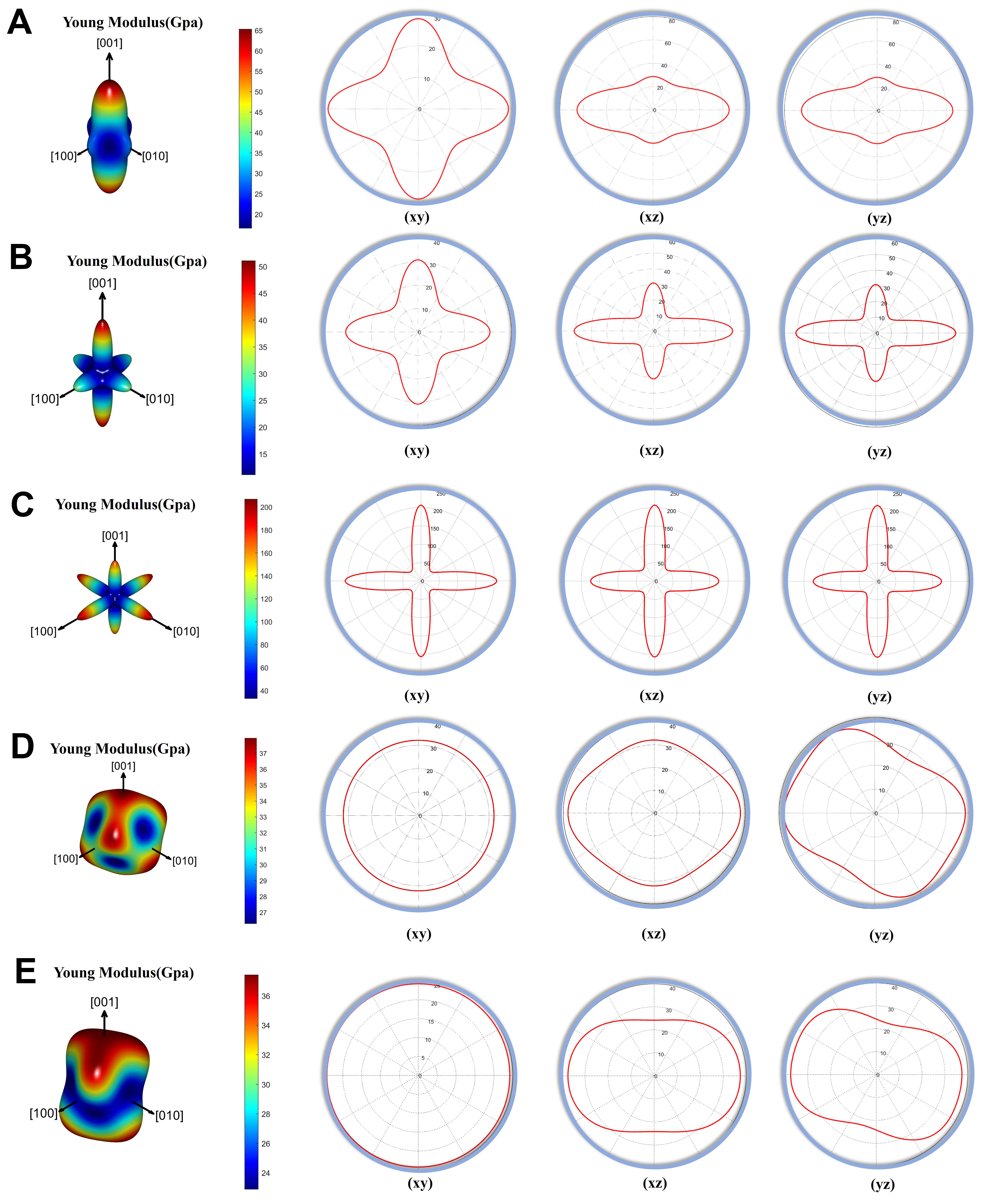
Figure 6. The directional dependence of E: (A) KGaSe2-I41/amd; (B) KGaTe2-I41/amd; (C) KInSe2-I41/amd; (D)KInTe2-R3̅m; (E)CsInTe2-R3̅m. And the construction of the corresponding system on 2D xy, xz, and yz projection planes. E: Young’s modulus.
After mechanical property screening, currently there are five potential infrared detection materials. In high-performance electronic devices, a smaller effective mass enhances electron mobility, thereby improving the switching speed and overall device performance. In optoelectronic materials, higher carrier mobility facilitates the efficient collection of photo-generated carriers, thereby enhancing the material’s photoresponse capability. The carrier mobility (μ) depends on the effective mass (m) and the relaxation time (τ), expressed as[64-67]:
Therefore, in the performance evaluation of infrared absorption materials, the effective mass (m*) of electrons and holes is a crucial physical parameter, as it directly affects carrier mobility and the optical response characteristics of the material. Specifically, the effective mass of electrons (me*) and holes (mh*) can be calculated using either the curvature approximation of the parabolic band structure or a numerical fitting approach[67]. The expression is given as follows:
where ℏ is the reduced Planck’s constant, E is the energy of the electronic state, and k is the wave vector in reciprocal space.
For a single isotropic and parabolic conduction band, the effective mass can be obtained from the curvature of the conduction band[68]. Among the five candidate materials, KGaSe2-I41/amd, KGaTe2-I41/amd, and KInSe2-I41/amd exhibit relatively low electron mobility, as shown in the table, with a decreasing trend in mobility. This also indicates that the In-Se bond in KInSe2-I41/amd exhibits stronger covalent characteristics compared to the Ga-Se bond in KGaTe2-I41/amd. Notably, KInSe2-I41/amd has both hole and electron effective masses smaller than 1, which is advantageous for infrared photodetectors. A smaller hole mass implies a longer carrier diffusion length, reducing non-radiative recombination losses and thereby enhancing the photoelectric conversion efficiency. Notably, as shown in Table 2, KInSe2-I41/amd exhibits both electron and hole effective masses below 1 m0, indicating a favorable balance for infrared photodetector applications. A smaller electron effective mass enhances electron transport, allowing photo-generated electrons to quickly reach the collecting electrode[69-71]. Meanwhile, a lower hole effective mass implies a longer carrier diffusion length, reducing non-radiative recombination losses and thereby improving photoelectric conversion efficiency.
Electronic effective mass, hole effective mass, and exciton binding energy for KGaSe2-I41/amd, KGaTe2-I41/amd, KInSe2-I41/amd, KInTe2-R3̅m, CsInTe2-R3̅m
| Compounds | Electron effective mass (me*) | Hole effective mass (mh*) | |
| KGaSe2-I41/amd | K - Г | 0.25 | 1.86 |
| K - M | 0.25 | 3.31 | |
| KGaTe2-I41/amd | K - Г | 0.23 | 1.71 |
| K - M | 0.23 | 1.82 | |
| KInSe2-I41/amd | K - Г | 0.18 | 0.19 |
| K - M | 1.5 | 0.51 | |
| KInTe2-R3̅m | K - Г | 0.25 | 0.39 |
| K - M | 0.74 | 4.13 | |
| CsInTe2-R3̅m | K - Г | 0.48 | 0.23 |
| K - M | 0.50 | 3.73 | |
Furthermore, in optoelectronic devices such as photodetectors, maintaining effective mass values within an optimal range is essential. If the electron effective mass is too small (e.g., below 0.1 m0), the resulting excessively high mobility may cause electrons to transit the active region too rapidly, reducing their probability of recombining with holes and thereby suppressing radiative recombination efficiency. Consequently, moderate and well-balanced effective masses for both electrons and holes are generally preferred, as they can simultaneously support efficient carrier transport and favorable recombination dynamics, which are critical for achieving high sensitivity and efficiency in infrared photodetection.
It should be emphasized that, in the present work, the calculated effective masses are not intended to provide a quantitative evaluation of carrier mobility, which would additionally require knowledge of carrier relaxation times and scattering mechanisms. Instead, the effective-mass analysis is used as an indicator of carrier transport potential, suggesting that the selected materials possess favorable transport characteristics under appropriate conditions. A comprehensive assessment of carrier mobility, including explicit relaxation-time calculations, is left for future studies.
As shown Figure 6, KGaSe2-I41/amd and KInSe2-I41/amd exhibit high bulk moduli (19.22 and 84.95 GPa, respectively), indicating strong resistance to compression and potential for long-term operational stability in optoelectronic devices. KInSe2-I41/amd (E = 80.79 GPa, G = 30.11 GPa) and CsInTe2-R3̅m (E = 29.560 GPa, G = 11.280 GPa) show superior stiffness and resistance to deformation.
According to the Pugh criterion (B/G > 1.75), all three materials are ductile. Although this implies excellent ductility, its low bulk and Young’s moduli suggest compromised mechanical stability. In contrast, KGaTe2-I41/amd and CsInTe2-R3̅m (B/G = 2.40 and 2.99, respectively) provide a more favorable trade-off between ductility and structural robustness. Positive Cauchy pressures confirm the dominance of ionic bonding in all structures, supporting their ductile behavior. Poisson’s ratios for the materials range from 0.32 to 0.36, consistent with typical values for semiconductors. The θD of KGaTe2-I41/amd (132.60 K) indicate strong thermal stability, beneficial for high-power optoelectronic applications. CsInTe2-R3̅m, with a lower θD (94.00 K), may experience more significant thermal expansion, limiting its use under high-temperature conditions. Elastic anisotropy, evaluated via the Zener factor and illustrated in Figure 6, reveals that none of the materials are elastically isotropic. KInSe2-I41/amd shows the most pronounced anisotropy, which may lead to direction-dependent mechanical performance. In contrast, CsInTe2-R3̅m exhibits moderate anisotropy, favorable for uniform mechanical response in flexible devices.
In summary, CsInTe2-R3̅m offers a desirable combination of ductility, thermal stability, and manageable anisotropy, making them promising candidates for flexible applications. KInSe2-I41/amd, while exhibiting excellent rigidity, requires further mechanical and thermal optimization for reliable use in flexible infrared detection systems.
In the band analysis section, 3 of 5 materials were found to exhibit direct bandgaps, which have better electronic transition efficiency compared with indirect bandgap materials, and all the bandgap values are shown in Figure 7. The following sections will provide a detailed investigation of the optical properties of KGaSe2-I41/amd, KGaTe2-I41/amd, KInSe2-I41/amd, KInTe2-R3̅m and CsInTe2-R3̅m.
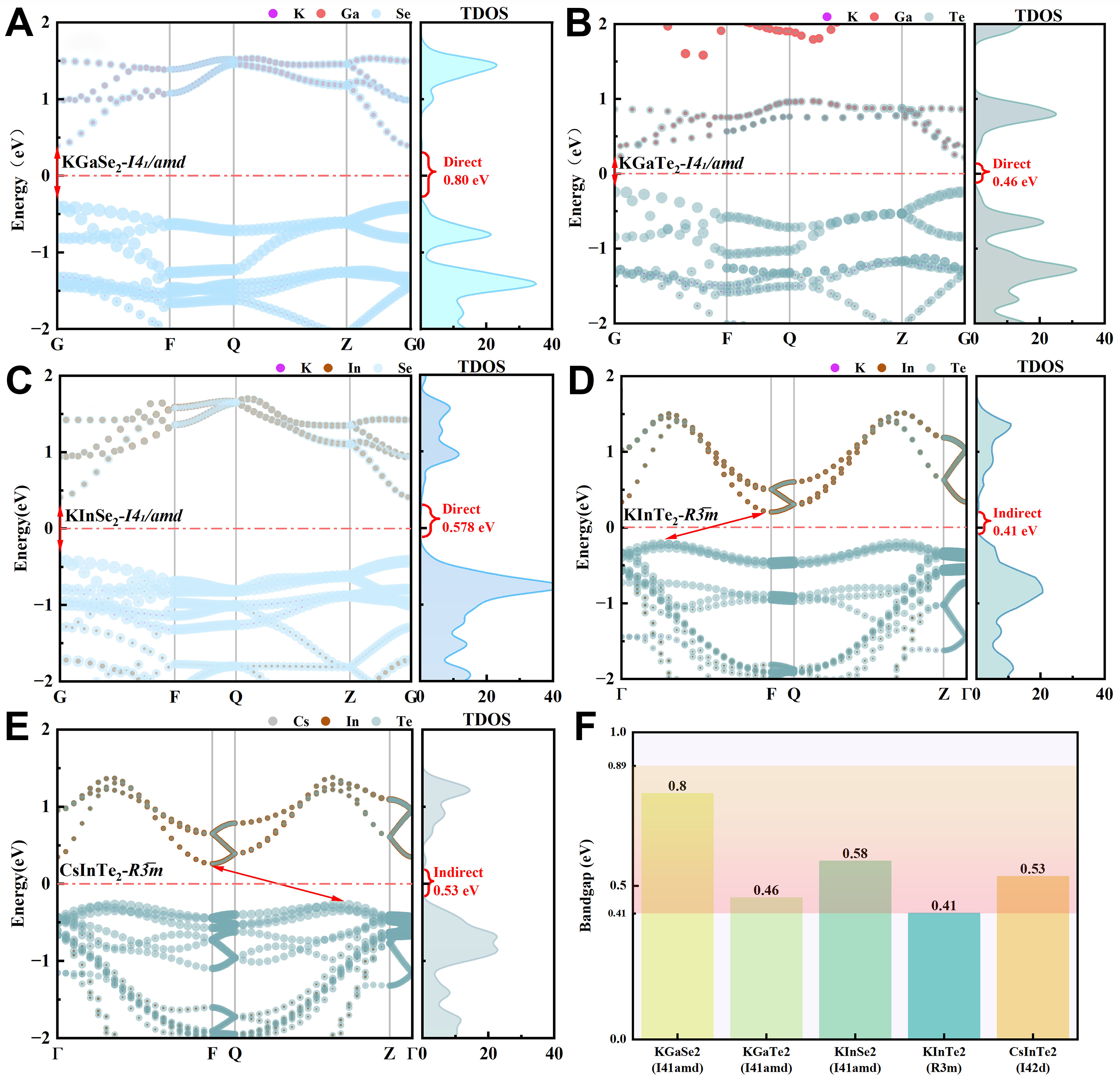
Figure 7. The band structures and TDOS of the (A) KGaSe2-I41/amd; (B) KGaTe2-I41/amd; (C) KInSe2-I41/amd; (D) KInTe2-R3̅m and (E) CsInTe2-R3̅m; (F) Bandgap data summary chart. The Fermi energy is set to zero. TDOS: Total density of states.
The analysis of the band structure and TDOS in the images reveals that different space groups have a significant impact on the band properties and electronic state distribution of materials. In the tetragonal crystal system, KGaSe2, KGaTe2, and KInSe2 with the I41/amd space group are all direct bandgap semiconductors, with the band extremum appearing at the same momentum space point, which is conducive to light absorption and photoelectric conversion. Among them, KGaSe2 has the highest bandgap (0.80 eV), while KGaTe2 has the lowest bandgap (0.46 eV), indicating that selenium (Se) has a greater influence on the band structure. Its TDOS shows that the electronic state distribution is relatively concentrated, which is suitable for infrared detection applications. Moreover, its TDOS shows that the electronic state distribution is relatively dispersed, which may improve the transport performance of photo-generated carriers.
The CsInTe2 and the KInTe2 of the R3̅m space group exhibits an indirect bandgap (0.525 and 0.409 eV), and the band extremum does not match in the momentum space. This will affect the optical transition and the efficiency of photoelectric conversion, but the longer carrier lifetime makes it advantageous in certain photoelectric applications. Its TDOS shows a gentler distribution of electronic states, suggesting better electronic transport performance. Overall, the I41/amd structure tends to form a direct bandgap, suitable for efficient photoelectric conversion; while the R3̅m structure may introduce an indirect bandgap, suitable for infrared detection applications with long carrier lifetime. Reasonable selection of the space group structure can optimize the band properties of the material, thereby enhancing the performance of optoelectronic devices.
A comparison between structures with the same chemical composition (CsInTe2) but different space groups highlight significant variations in bandgaps and physical properties. To gain microscopic insights, partial density of states (PDOS) was conducted for the five selected materials.
From the Figure 8, it can be observed that the chalcogen atoms (Se and Te) contribute dominantly to the outermost orbital states, while the A-site atoms, including K and Cs, contribute the least. In particular, Cs exhibits an almost negligible contribution. At the VBM, the p orbitals of C-site atoms play a prominent role. Since the VBM is the starting point for electronic transitions in semiconductors and represents the location where photo-generated electron-hole pairs form, this indicates that the C-site atoms have a significant impact on hole effective mass and carrier mobility. Furthermore, in terms of bonding, the C-site atoms form strongly polar covalent bonds with the B-site atoms. Notably, in the high-energy region of the conduction band, different bonding characteristics can be observed. In KGaSe2-I41/amd, the conduction band is primarily formed by the overlap between Ga 4p orbitals and Se 4s orbitals. In contrast, in KInTe2-R3̅m, and CsInTe2-R3̅m, the conduction band is mainly composed of the overlap between In 5p orbitals and Te 5s orbitals. This strong orbital overlap further confirms the covalent nature of the bonding between B-site and C-site atoms.
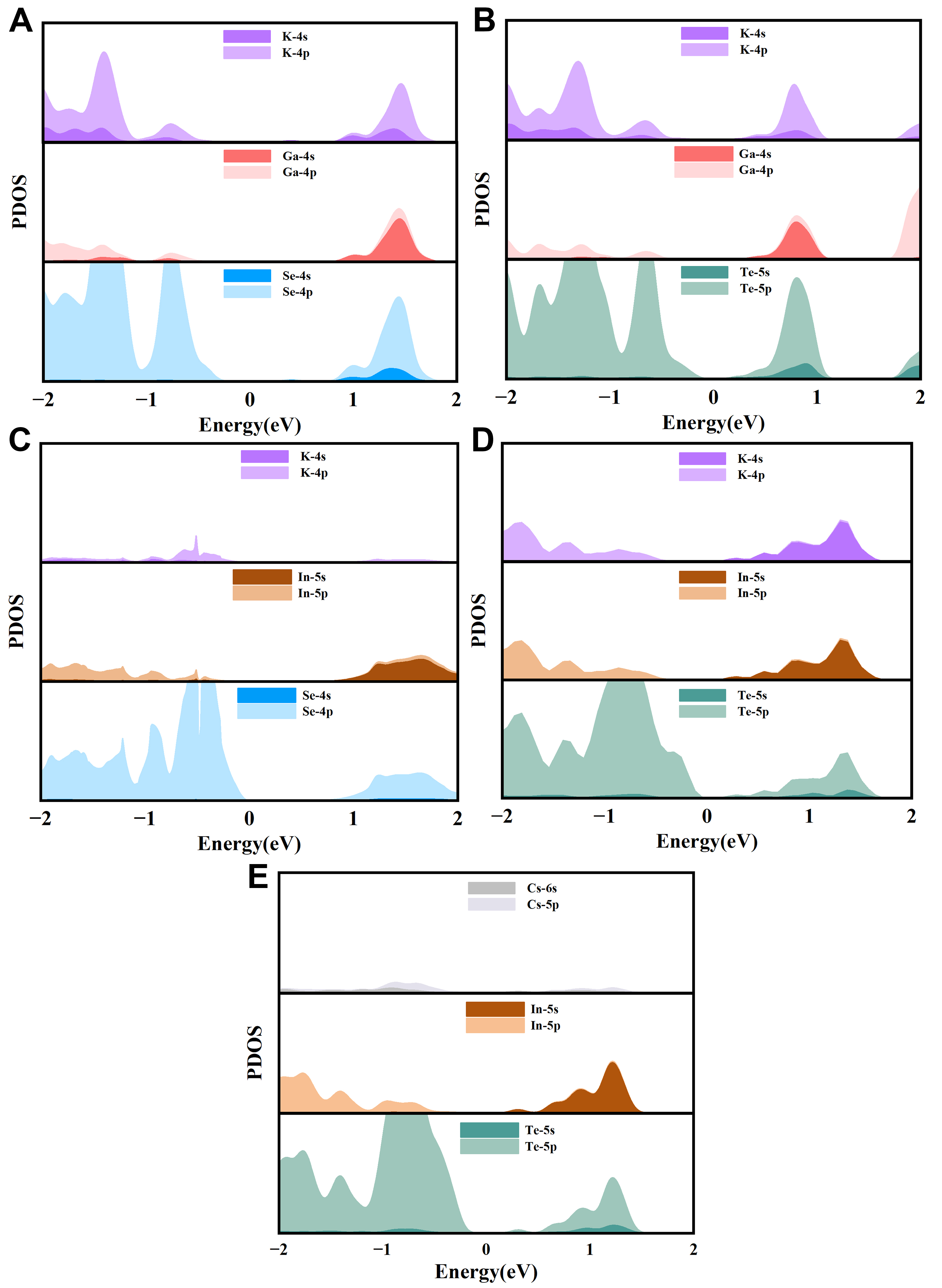
Figure 8. PDOS for six systems: (A) KGaSe2-I41/amd; (B) KGaTe2-I41/amd; (C) KInSe2-I41/amd; (D) KInTe2-R3̅m; and (E) CsInTe2-R3̅m. In the calculations, the Fermi level (E_F) is set to 0 eV. The abscissa represents the energy relative to the Fermi level (unit: eV), and the ordinate denotes the DOS (unit: states/eV). Different lines in the figure correspond to the orbital contributions of different elements (e.g., Se 4p, Ga 4p and so on). PDOS: Projected density of states; DOS: density of states; EF: Fermi level; eV: electron volt.
To address the systematic band gap underestimation of the PBE functional, we further validated the band gaps of the five final candidates using the HSE06 hybrid functional (a standard approach for accurate semiconductor band gap prediction). The results are summarized in Supplementary Table 7: KGaSe2-I41/amd (1.59 eV), KGaTe2-I41/amd (1.08 eV), KInSe2-I41/amd (1.55 eV), KInTe2- R3̅m (0.92 eV), and CsInTe2- R3̅m (1.03 eV). Importantly, HSE06 calculations confirm that the bandgap characteristics of all five candidates remain unchanged compared to the PBE results, and all HSE06-corrected band gaps fall within or near the SWIR-relevant range (0.4-1.55 eV, 0.8-3.0 μm), confirming the suitability of these candidates for SWIR detection. Specifically, KGaTe2-I41/amd, KInTe2-R3̅m, and CsInTe2-R3̅m are within the conventional SWIR range (0.92-1.08 eV), while KGaSe2- I41/amd and KInSe2-I41/amd lie in the near-infrared (NIR)-SWIR transition region (~0.78-0.80 μm), which is widely included in broadband SWIR detection systems[72]. As a representative example, the HSE06 band structure of KGaSe2 is shown in Supplementary Figure 5, which explicitly demonstrates that the direct bandgap character at the Γ point is preserved at the hybrid-functional level. The remaining four candidates exhibit the same qualitative behavior in their HSE06 band-edge characteristics; therefore, only one representative band structure is presented for clarity.
To ensure that the 5 candidates identified are dynamically stable and are viable to be experimentally synthesized, we also calculate AIMD simulations specifically, as shown in Figure 4B. The energy fluctuations of the material remained within a narrow range, indicating its thermodynamic stability at 300 K. Figure 9A shows that the formation energies of all candidate materials are negative, indicating their thermodynamic stability; the AIMD simulation results in Figure 9B demonstrate small energy fluctuations of the materials at 300 K, further verifying their thermal stability. The results from formation energy analysis and molecular dynamics simulations further confirm that this material possesses excellent stability and manufacturability.
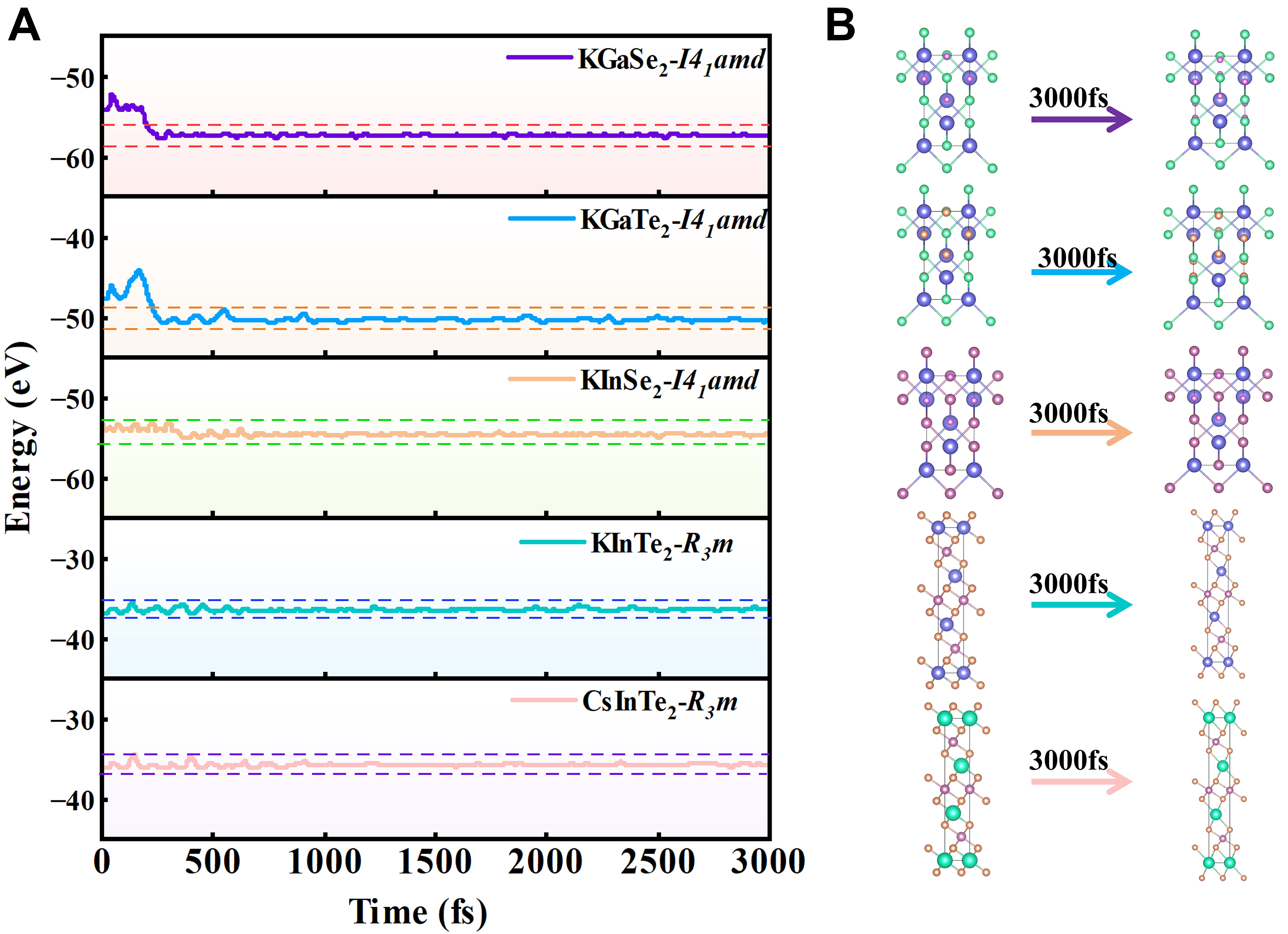
Figure 9. (A) Total energy evolution as a function of simulation time obtained from AIMD simulations performed at finite temperature for the corresponding candidate structures; (B) Representative atomic configurations of the candidate structures before and after 3,000 fs of AIMD simulation. The AIMD simulations are used to assess short-time local structural robustness rather than to establish definitive thermodynamic stability. fs: Femtosecond; AIMD: Ab initio molecular dynamics.
Note that PBE was used only for initial HTS (rapidly excluding metallic/wide-gap systems) and relative optical property analysis (reliable for trend prediction[73], while the final candidate validation relies on HSE06 band gaps, AIMD-based dynamical stability, and elastic constant-verified mechanical stability.
CONCLUSIONS
In summary, this work establishes an integrated HTS framework that synergizes ML with DFT to expedite the discovery of SWIR detection materials. By leveraging a curated database of I-X-VI chalcogenides and optimizing ML regression models, the framework efficiently identifies promising candidates with tailored bandgaps and desirable electronic properties, with XGBR proving to be the most robust predictor. DFT validation confirms the reliability of the screening pipeline and highlights KGaSe2 as a particularly promising candidate due to its optimal bandgap and superior carrier transport characteristics. This full-chain design paradigm offers a scalable and interpretable alternative to conventional discovery methods. Future research will expand this framework to broader chemical spaces and advanced ML architectures, facilitating the rapid development of functional materials for next-generation optoelectronic devices.
DECLARATIONS
Acknowledgements
We are grateful for the valuable discussions and computational resources provided by the Beijing Computational Science Research Center (CSRC), and acknowledge the support from the Talent Hub for “AI+ New Materials” Basic Research.
Authors’ contributions
Conceptualization: Guan, X.; Zhang, Y. (Yanan); Zhang, F.; Zhang, Y. (Yanchao); Gao, H.
Data curation: Guan, X.; Zhang, Y. (Yanan); Han, S.; Xiong, C.; Chen, C.
Formal analysis: Zhang, Y. (Yanan); Chen, C.; Zhang, F.; Zhang, Y. (Yanchao); Gao, H.
Funding acquisition: Guan, X.
Investigation: Zhang, Y. (Yanan); Han, S.
Methodology: Guan, X.; Zhang, Y. (Yanan); Chen, C.; Zhang, F.; Zhang, Y. (Yanchao); Gao, H.; Zhou, F.; Guan, P.; Lu, P.
Software: Zhang, Y. (Yanan)
Supervision: Guan, X.; Zhou, F.; Guan, P.; Lu, P.
Validation: Guan, X.; Zhang, F.; Zhang, Y. (Yanan); Gao, H.
Writing - original draft: Zhang, Y. (Yanan); Han, S.
Writing - review & editing: Zhang, Y. (Yanan); Han, S.; Xiong, C.; Yang, Y.; Chen, C.; Zhou, F.; Guan, P.; Lu, P.
Availability of data and materials
The original contributions presented in this study are included in the Supplementary Materials. Further inquiries can be directed to the corresponding authors.
AI and AI-assisted tools statement
Not applicable.
Financial support and sponsorship
This work was supported financially by the National Key Research and Development Program Projects of China (No. 2022YFB3204203) and Infrared Detection National Key Laboratory Open Project (No. IRDT-24-02).
Conflicts of interest
Zhang, F.; Zhang, Y. (Yanchao); and Gao, H. are affiliated with Ningbo Weiyuan Optoelectronic Research Institute Co., Ltd. The other authors declared that there are no conflicts of interest.
Ethical approval and consent to participate
Not applicable.
Consent for publication
Not applicable.
Copyright
© The Author(s) 2026.
Supplementary Materials
REFERENCES
2. Fu, L.; He, Y.; Zheng, J.; et al. Tex Se1-x photodiode shortwave infrared detection and imaging. Adv. Mater. 2023, 35, e2211522.
3. Amani, M.; Tan, C.; Zhang, G.; et al. Solution-synthesized high-mobility tellurium nanoflakes for short-wave infrared photodetectors. ACS. Nano. 2018, 12, 7253-63.
4. Guan, X.; Yu, X.; Periyanagounder, D.; et al. Recent progress in short- to long-wave infrared photodetection using 2D materials and heterostructures. Adv. Opt. Mater. 2021, 9, 2001708.
5. Zulfiqar, M. W.; Nisar, S.; Dastgeer, G.; et al. 2D material-based infrared photodetectors: recent progress, challenges, and perspectives. Nanoscale 2025, 17, 17881-918.
6. Ji, X.; Lu, C.; Cheng, L. Recent advances in two-dimensional materials in infrared photodetectors (invited). Infrared. Laser. Eng. 2022, 51, 20220065.
7. Wu, Z.; Ou, Y.; Cai, M.; Wang, Y.; Tang, R.; Xia, Y. Short-wave infrared photodetectors and imaging sensors based on lead chalcogenide colloidal quantum dots. Adv. Opt. Mater. 2023, 11, 2201577.
9. Kirklin, S.; Saal, J. E.; Meredig, B.; et al. The open quantum materials database (OQMD): assessing the accuracy of DFT formation energies. npj. Comput. Mater. 2015, 1, 15010.
10. Curtarolo, S.; Setyawan, W.; Wang, S.; et al. AFLOWLIB.ORG: a distributed materials properties repository from high-throughput Ab initio calculations. Comput. Mater. Sci. 2012, 58, 227-35.
11. Jain, A.; Voznyy, O.; Sargent, E. H. High-throughput screening of lead-free perovskite-like materials for optoelectronic applications. J. Phys. Chem. C. 2017, 121, 7183-7.
12. Li, Y.; Yang, K. High-throughput computational design of organic-inorganic hybrid halide semiconductors beyond perovskites for optoelectronics. Energy. Environ. Sci. 2019, 12, 2233-43.
13. Kuang, Z.; Liu, S.; Li, X.; et al. Topotactically constructed nickel-iron (oxy)hydroxide with abundant in-situ produced high-valent iron species for efficient water oxidation. J. Energy. Chem. 2021, 57, 212-8.
14. Wang, V.; Tang, G.; Liu, Y. C.; et al. High-throughput computational screening of two-dimensional semiconductors. J. Phys. Chem. Lett. 2022, 13, 11581-94.
15. Jacobs, R.; Liu, J.; Abernathy, H.; Morgan, D. Machine learning design of perovskite catalytic properties. Adv. Energy. Mater. 2024, 14, 2303684.
16. Ding, R.; Chen, J.; Chen, Y.; Liu, J.; Bando, Y.; Wang, X. Unlocking the potential: machine learning applications in electrocatalyst design for electrochemical hydrogen energy transformation. Chem. Soc. Rev. 2024, 53, 11390-461.
17. Lu, B.; Xia, Y.; Ren, Y.; et al. When machine learning meets 2D materials: a review. Adv. Sci. 2024, 11, e2305277.
18. Tameh, M. S.; Coropceanu, V.; Coen, A. G.; Pyun, J.; Lichtenberger, D. L.; Brédas, J. L. High-throughput computational screening of hydrocarbon molecules for long-wavelength infrared imaging. ACS. Mater. Lett. 2024, 6, 4371-8.
19. Sun, S.; Hartono, N. T.; Ren, Z. D.; et al. Accelerated development of perovskite-inspired materials via high-throughput synthesis and machine-learning diagnosis. Joule 2019, 3, 1437-51.
20. Wang, R.; Yu, H.; Zhong, Y.; Xiang, H. Identifying direct bandgap silicon structures with high-throughput search and machine learning methods. J. Phys. Chem. C. 2024, 128, 12677-85.
21. Hong, W.; Yuan, J.; Mao, Y. Janus halogenated silicene for photocatalytic and photovoltaic applications: a machine learning combined with first-principles study. J. Phys. Chem. C. 2024, 128, 14282-93.
22. Sa, B.; Hu, R.; Zheng, Z.; et al. High-throughput computational screening and machine learning modeling of Janus 2D III-VI van der Waals heterostructures for solar energy applications. Chem. Mater. 2022, 34, 6687-701.
23. Li, Y.; Yang, J.; Zhao, R.; et al. Design of organic-inorganic hybrid heterostructured semiconductors via high-throughput materials screening for optoelectronic applications. J. Am. Chem. Soc. 2022, 144, 16656-66.
24. Hu, W.; Zhang, L.; Pan, Z. Designing two-dimensional halide perovskites based on high-throughput calculations and machine learning. ACS. Appl. Mater. Interfaces. 2022, 14, 21596-604.
25. Ma, X.; Lewis, J. P.; Yan, Q.; Su, G. Accelerated discovery of two-dimensional optoelectronic octahedral oxyhalides via high-throughput Ab initio calculations and machine learning. J. Phys. Chem. Lett. 2019, 10, 6734-40.
26. Wu, Q.; Kang, L.; Lin, Z. A machine learning study on high thermal conductivity assisted to discover chalcogenides with balanced infrared nonlinear optical performance. Adv. Mater. 2024, 36, e2309675.
27. Chen S.; Li T.; Zhang Y.; Long T.; Fortunato N. M.; Liang F.; Dai M.; Shen J.; Wolverton C.; Zhang H. Accelerated screening of ternary chalcogenides for high-performance optoelectronic materials. arXiv 2023, arXiv:2305.02634. Available online: https://arxiv.org/abs/2305.02634. (accessed 21 April 2026).
28. Teng, H. Y.; Yang, J. X. Optical response modulation of AgBiS2 through order-disordered transition. Technol. Dev. Chem. Ind. 2023, 52, 1-4.
29. Ruan, C.; Yang, S. Y.; Gu, Z. C.; et al. Ideal weyl semimetals in the chalcopyrites CuTlSe2, AgTlTe2, AuTlTe2, and ZnPbAs2. Phys. Rev. Lett. 2016, 116, 226801.
30. Mesquita, L. V.; Mansour, D. E.; Gebhardt, P.; Pitta Bauermann, L. Scanning acoustic microscopy analysis of the mechanical properties of polymeric components in photovoltaic modules. Eng. Rep. 2020, 2, e12222.
31. Lin, S.; Ma, Z.; Ji, X.; et al. Efficient large-area (81 cm2) ternary copper halides light-emitting diodes with external quantum efficiency exceeding 13% via host-guest strategy. Adv. Mater. 2024, 36, e2313570.
32. Kim, K.; Ward, L.; He, J.; Krishna, A.; Agrawal, A.; Wolverton, C. Machine-learning-accelerated high-throughput materials screening: discovery of novel quaternary Heusler compounds. Phys. Rev. Materials. 2018, 2, 123801.
33. Wada, T. CuInSe2 and related I-III-VI2 chalcopyrite compounds for photovoltaic application. Jpn. J. Appl. Phys. 2021, 60, 080101.
34. Zhang, T.; Yang, Y.; Liu, D.; et al. High efficiency solution-processed thin-film Cu(In,Ga)(Se,S)2 solar cells. Energy. Environ. Sci. 2016, 9, 3674-81.
35. García‐hemme, E.; Caudevilla, D.; Algaidy, S.; et al. On the optoelectronic mechanisms ruling Ti‐hyperdoped Si photodiodes. Adv. Electron. Mater. 2022, 8, 2100788.
36. Obulesu O.; Mahendra M.; Thrillokreddy M. Machine learning techniques and tools: a survey. In 2018 International Conference on Inventive Research in Computing Applications (ICIRCA), IEEE: 2018; pp 605-611.
37. El Mrabet M. A.; El Makkaoui K.; Faize A. Supervised machine learning: a survey. In 2021 4th International Conference on Advanced Communication Technologies and Networking (CommNet), IEEE: 2021; pp 1-10.
38. Smajić, A.; Grandits, M.; Ecker, G. F. Using Jupyter Notebooks for re-training machine learning models. J. Cheminform. 2022, 14, 54.
39. Pedregosa F, Varoquaux G, Gramfort A, et al. Scikit-learn: machine learning in Python. J Mach Learn Res 2011;12:2825-30. https://jmlr.org/papers/v12/pedregosa11a.html (accessed 2026-04-21).
40. Kresse, G.; Furthmüller, J. Efficient iterative schemes for Ab initio total-energy calculations using a plane-wave basis set. Phys. Rev. B. Condens. Matter. 1996, 54, 11169-86.
41. Segall, M. D.; Lindan, P. J. D.; Probert, M. J.; et al. First-principles simulation: ideas, illustrations and the CASTEP code. J. Phys. Condens. Matter. 2002, 14, 2717-44.
42. Setyawan, W.; Curtarolo, S. High-throughput electronic band structure calculations: challenges and tools. Comput. Mater. Sci. 2010, 49, 299-312.
43. Huck P.; Jain A.; Gunter D.; Winston D.; Persson K. A. A community contribution framework for sharing materials data with Materials Project. In 2015 IEEE 11th International Conference on e-Science, IEEE: 2015; pp 535-541.
44. Cheng, J.; Wu, S.; Yan, X.; et al. Growth and characterization of AgBiS2 bulk single crystals for near-infrared detectors. Cryst. Growth. Des. 2024, 24, 8445-53.
45. Woods-Robinson, R.; Han, Y.; Zhang, H.; et al. Wide band gap chalcogenide semiconductors. Chem. Rev. 2020, 120, 4007-55.
46. Fatmi, M.; Bouferrache, K.; Ghebouli, M. A.; Ghebouli, B.; Alomairy, S.; Alanazi, F. K. Investigation of structural, elastic, electronic, optical, and thermoelectric properties of LiInS2 and LiInTe2 for optoelectronic and energy conversion. Sci. Rep. 2025, 15, 27859.
47. Khalfin, S.; Bekenstein, Y. Advances in lead-free double perovskite nanocrystals, engineering band-gaps and enhancing stability through composition tunability. Nanoscale 2019, 11, 8665-79.
48. Miah, M. H.; Khandaker, M. U.; Rahman, M. B.; Nur-E-Alam, M.; Islam, M. A. Band gap tuning of perovskite solar cells for enhancing the efficiency and stability: issues and prospects. RSC. Adv. 2024, 14, 15876-906.
49. Yang, J. N.; Chen, T.; Ge, J.; et al. High color purity and efficient green light-emitting diode using perovskite nanocrystals with the size overly exceeding bohr exciton diameter. J. Am. Chem. Soc. 2021, 143, 19928-37.
50. Lin, K.; Xing, J.; Quan, L. N.; et al. Perovskite light-emitting diodes with external quantum efficiency exceeding 20 per cent. Nature 2018, 562, 245-8.
51. Yang, X.; Zhang, X.; Deng, J.; et al. Efficient green light-emitting diodes based on quasi-two-dimensional composition and phase engineered perovskite with surface passivation. Nat. Commun. 2018, 9, 570.
52. Hoang, K.; Mahanti, S. D. Atomic and electronic structures of I-V-VI2 ternary chalcogenides. J. Sci. Adv. Mater. Devices. 2016, 1, 51-6.
53. Tan, C.; Amani, M.; Zhao, C.; et al. Evaporated Sex Te1-x thin films with tunable bandgaps for short-wave infrared photodetectors. Adv. Mater. 2020, 32, e2001329.
54. Chen, Y.; Zheng, Y.; Wang, J.; et al. Ultranarrow-bandgap small-molecule acceptor enables sensitive SWIR detection and dynamic upconversion imaging. Sci. Adv. 2024, 10, eadm9631.
55. Bartel, C. J.; Trewartha, A.; Wang, Q.; Dunn, A.; Jain, A.; Ceder, G. A critical examination of compound stability predictions from machine-learned formation energies. npj. Comput. Mater. 2020, 6, 97.
56. Wang, Q.; Xu, B.; Sun, J.; et al. Direct band gap silicon allotropes. J. Am. Chem. Soc. 2014, 136, 9826-9.
57. Agrawal G. P.; Dutta N. K. Recombination mechanisms in semiconductors. In Semiconductor Lasers; Springer: Boston, MA, 1993.
58. Wang, S.; Zhang, Z.; Chen, C.; et al. Achieve near-infrared absorption in Cs3Sb2Br9 through 3d orbital energy level splitting to construct high-performance intermediate band solar cells. Chem. Eng. J. 2025, 504, 158638.
59. Wang, S.; Chen, C.; Shi, S.; et al. Flexibility potential of Cs2BX6 (B = Hf, Sn, Pt, Zr, Ti; X = I, Br, Cl) with application in photovoltaic devices and radiation detectors. J. Energy. Chem. 2024, 95, 271-87.
60. Fadaly, E. M. T.; Dijkstra, A.; Suckert, J. R.; et al. Direct-bandgap emission from hexagonal Ge and SiGe alloys. Nature 2020, 580, 205-9.
61. Sarritzu, V.; Sestu, N.; Marongiu, D.; et al. Direct or indirect bandgap in hybrid lead halide perovskites? Adv. Opt. Mater. 2018, 6, 1701254.
62. Khandy, S. A.; Yousuf, S.; Gupta, D. C. Structural, Magneto‐electronic, mechanical, and thermophysical properties of double perovskite Ba2ZnReO6. Phys. Status. Solidi. B. 2019, 256, 1800625.
63. Yang, K.; Wan, R.; Zhang, Z.; Lei, Y.; Tian, G. First-principle investigation on the thermoelectric and electronic properties of HfCoX (X=As, Sb, Bi) half-Heusler compounds. J. Solid. State. Chem. 2022, 314, 123386.
64. Poncé, S.; Li, W.; Reichardt, S.; Giustino, F. First-principles calculations of charge carrier mobility and conductivity in bulk semiconductors and two-dimensional materials. Rep. Prog. Phys. 2020, 83, 036501.
65. Su, L.; Shi, H.; Wang, S.; et al. Enhancing carrier mobility and seebeck coefficient by modifying scattering factor. Adv. Energy. Mater. 2023, 13, 2300312.
66. Qian, X.; Zhang, X.; Guo, H.; et al. Enhancing thermoelectric performance of n-type AgBi3S5 through synergistically optimizing the effective mass and carrier mobility. J. Materiomics. 2023, 9, 874-81.
67. Xiao, Y.; Liu, W.; Zhang, Y.; et al. Rationally optimized carrier effective mass and carrier density leads to high average ZT value in n-type PbSe. J. Mater. Chem. A. 2021, 9, 23011-8.
68. Hautier, G.; Miglio, A.; Waroquiers, D.; Rignanese, G.; Gonze, X. How does chemistry influence electron effective mass in oxides? A high-throughput computational analysis. Chem. Mater. 2014, 26, 5447-58.
69. Sun, Q.; Jiang, T.; Ou, Q.; Peng, Q.; Shuai, Z. Influence of intermolecular packing on light emitting efficiency and carrier-mobility of organic semiconductors: theoretical descriptor for molecular design. Adv. Opt. Mater. 2023, 11, 2202621.
70. Xie, M.; Li, T.; Liu, C.; et al. Realizing highly efficient blue electrofluorescence by optimized hybridized local and charge transfer state and balanced carrier mobilities. Chem. Eng. J. 2023, 472, 144950.
71. Ye, G. D.; Ding, R.; Li, S. H.; et al. Single-crystalline hole-transporting layers for efficient and stable organic light-emitting devices. Light. Sci. Appl. 2024, 13, 136.
Cite This Article
How to Cite
Download Citation
Export Citation File:
Type of Import
Tips on Downloading Citation
Citation Manager File Format
Type of Import
Direct Import: When the Direct Import option is selected (the default state), a dialogue box will give you the option to Save or Open the downloaded citation data. Choosing Open will either launch your citation manager or give you a choice of applications with which to use the metadata. The Save option saves the file locally for later use.
Indirect Import: When the Indirect Import option is selected, the metadata is displayed and may be copied and pasted as needed.
About This Article
Copyright

Data & Comments
Data
0


Comments
Comments must be written in English. Spam, offensive content, impersonation, and private information will not be permitted. If any comment is reported and identified as inappropriate content by OAE staff, the comment will be removed without notice. If you have any queries or need any help, please contact us at [email protected].