

fig2
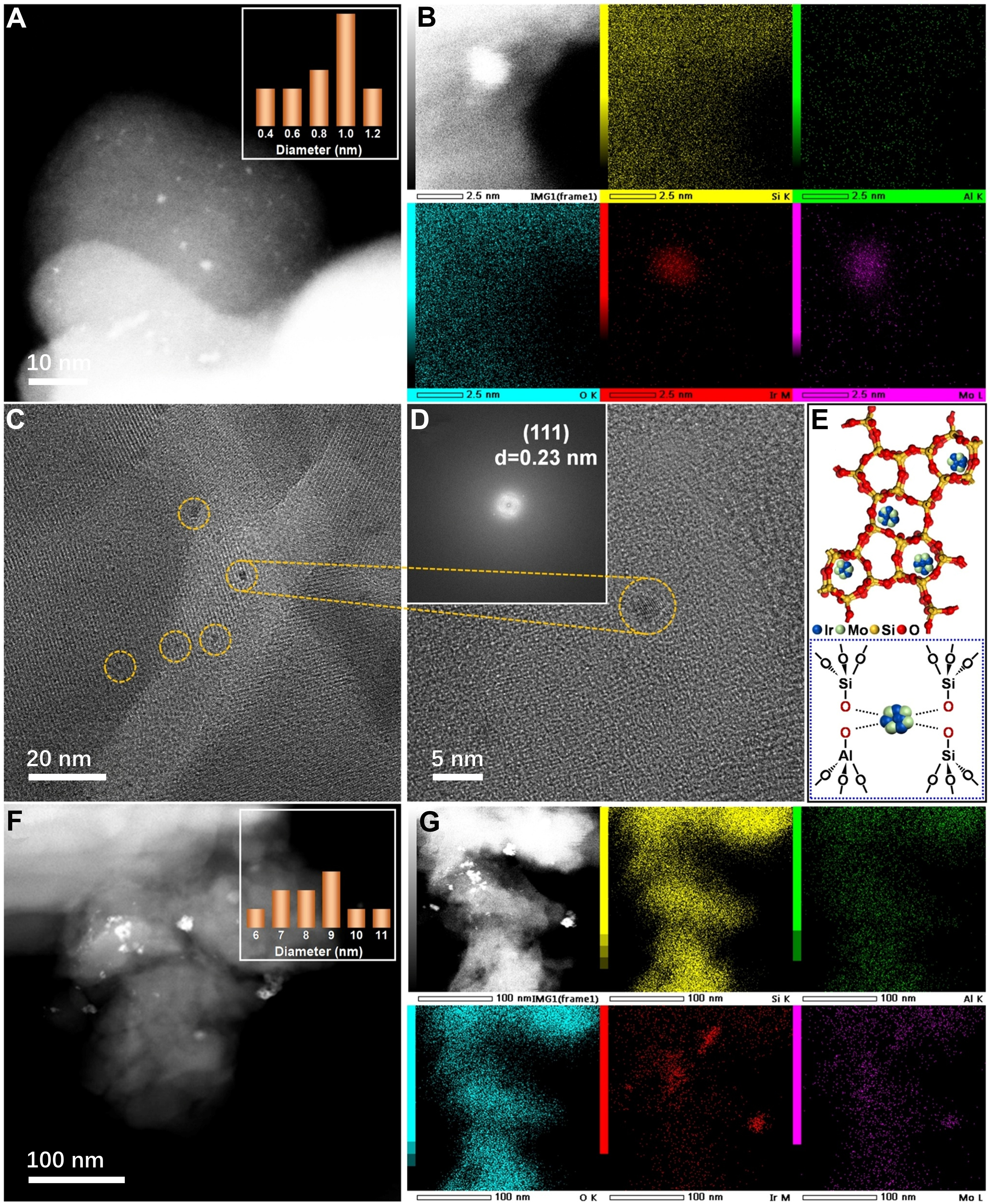
Figure 2. (A and B) TEM image and the corresponding EDS mapping images of Si, Al, O, Ir, Mo in Ir-Mo@Z5, (C and D) AC HAADF-STEM images of Ir-Mo@Z5, (E) structure diagram of Ir-Mo@Z5, and (F and G) TEM image and the corresponding EDS mapping images of Si, Al, O, Ir, Mo of Ir-Mo/Z5. TEM: Transmission electron microscopy; EDS: energy-dispersive X-ray spectroscopy; AC HAADF-STEM: aberration-corrected high-angle annular dark-field scanning transmission electron microscopy.

