


fig4
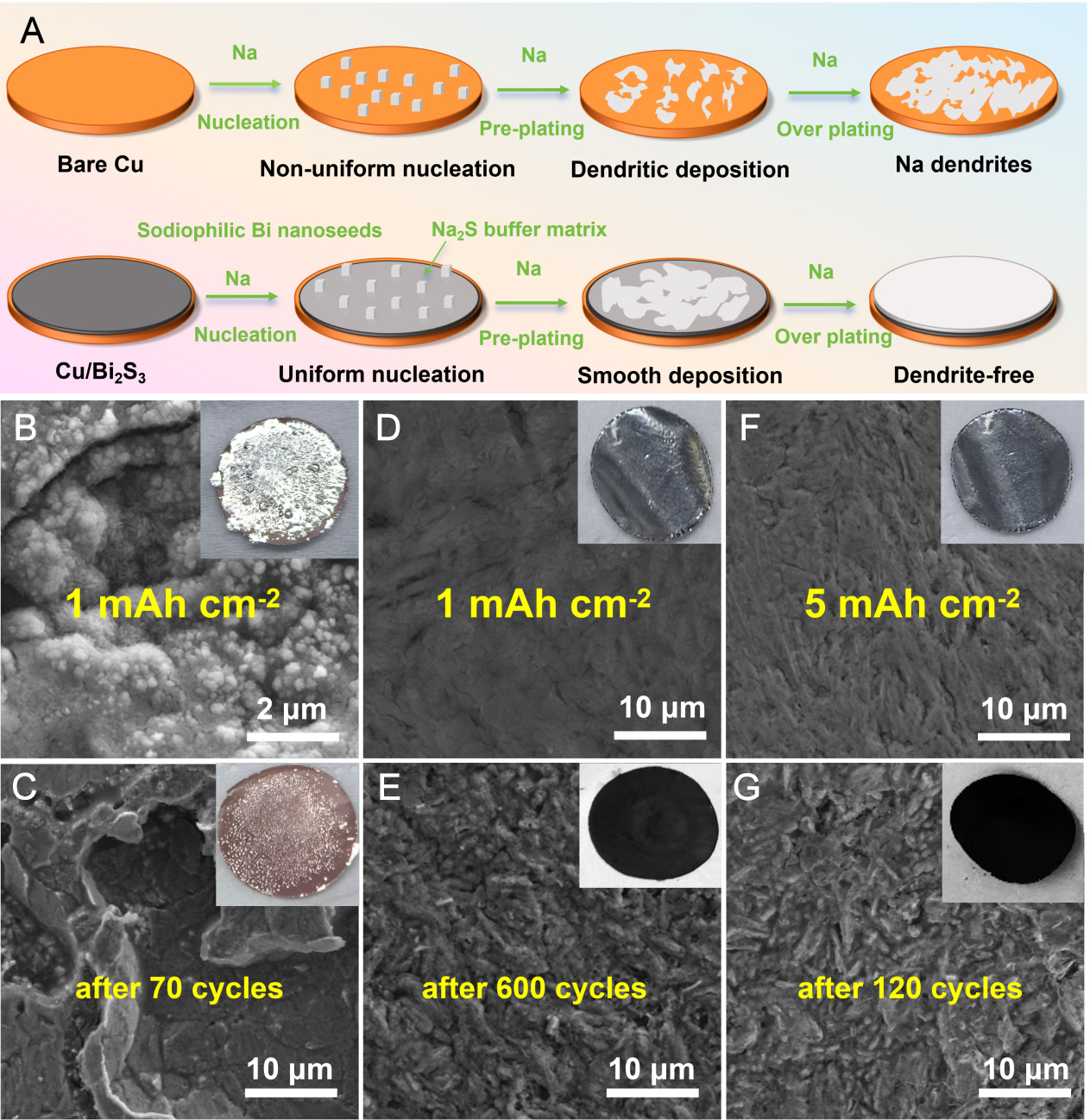
Figure 4. (A) Scheme illustrating the distinct Na plating behaviors on bare Cu and Bi2S3@Cu substrates; (B and C) Ex-situ SEM images of the bare Cu substrate after Na plating (B) and stripping (C) at 1 mA cm-2 with 1 mAh cm-2 after 70 cycles; (D-G) Ex-situ SEM images of the Bi2S3@Cu substrate after Na plating (D and F) and stripping (E and G) at 1 mA cm-2 with 1 mAh cm-2 (D and E) after 600 cycles and at


