


fig6
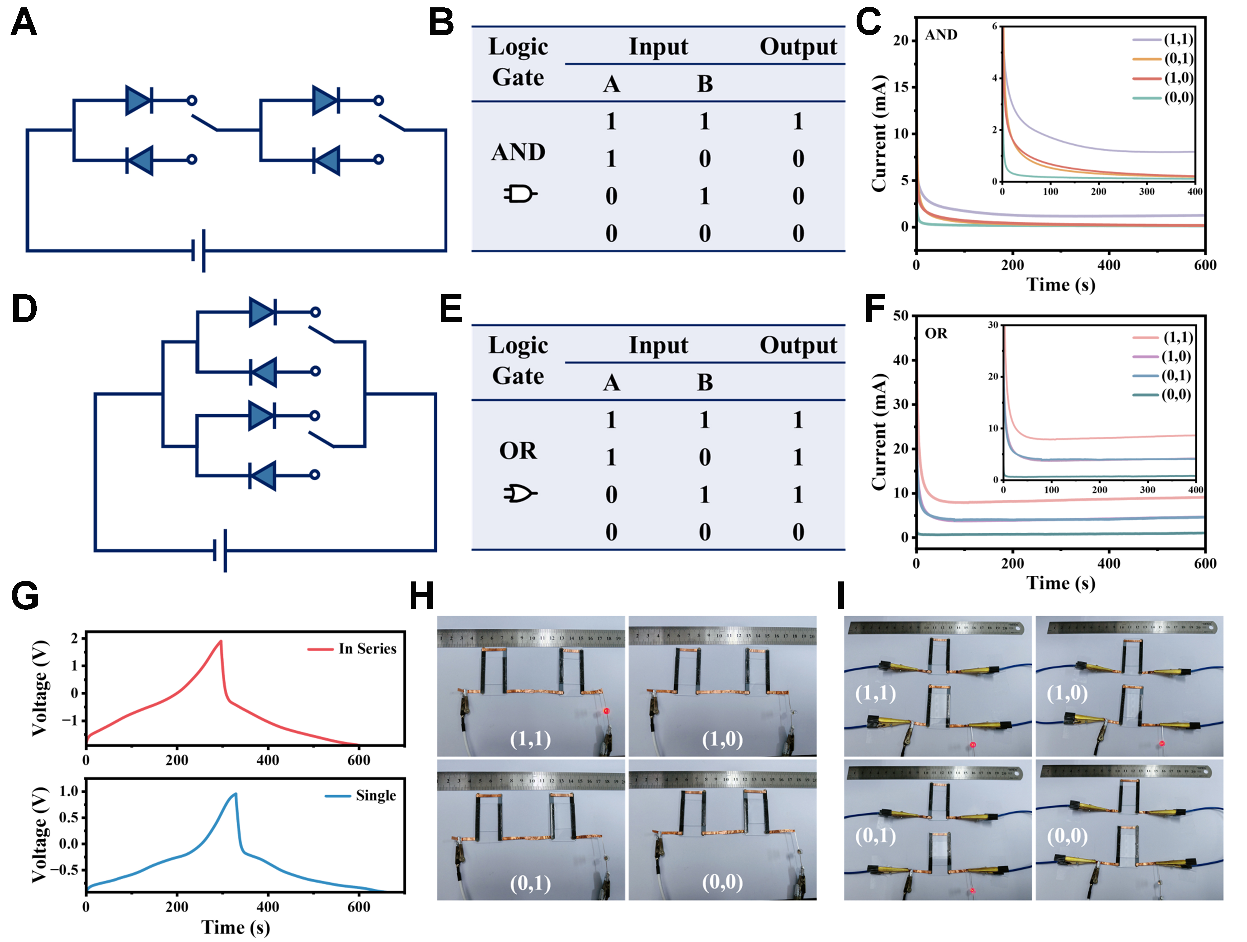
Figure 6. “AND” and “OR” logic gates based on CAPodes. (A-C) Schematic diagram (A), corresponding truth table (B), and output signals of an “AND” logic gate circuit (C); (D-F) Schematic diagram (D), corresponding truth table (E), and output signals of an “OR” logic gate circuit (F); (G) GCD curves of one single and two CAPodes connected in series; (H and I) Photographs by a digital camera of an “AND” gate (H) and an “OR” gate to switch an LED (I). GCD: Galvanostatic charge–discharge; LED: light emitting diode.


