

fig4
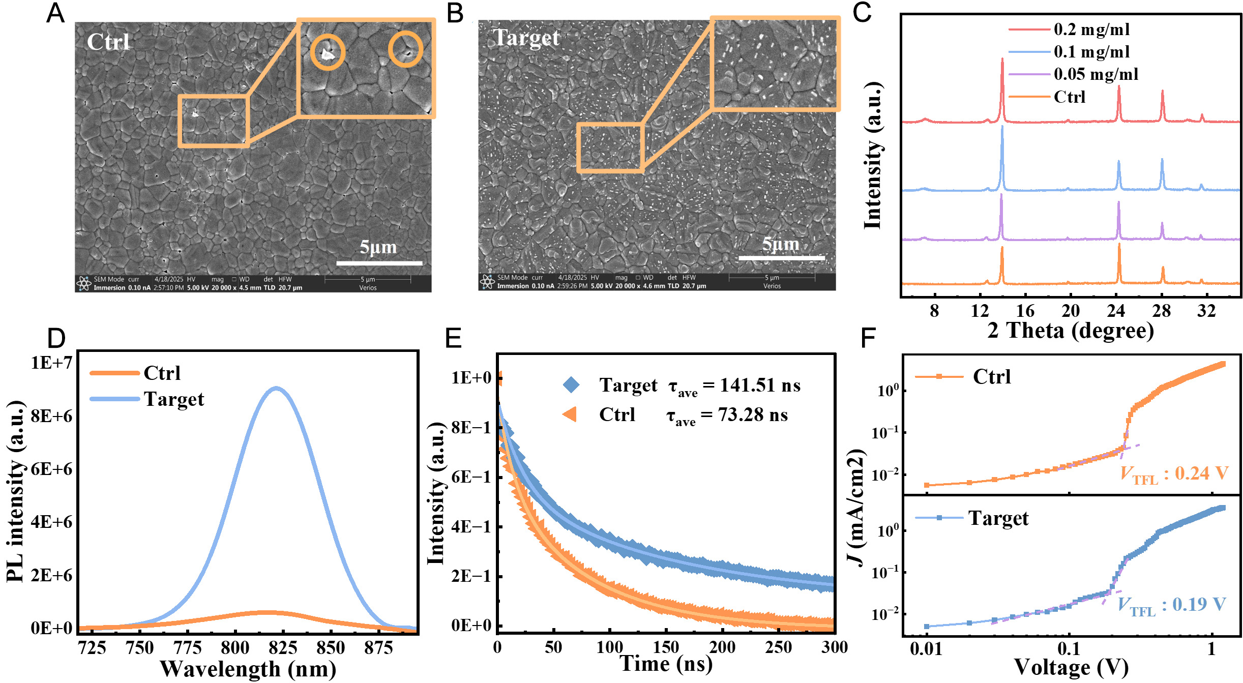
Figure 4. Top-view scanning electron microscopy (SEM) results for (A) the control sample and (B) the target film; (C) XRD patterns of FAPbI3 films treated with varying FTAC concentrations; PL (D) and TRPL (E) spectra of pristine and FTAC-treated perovskite layers; (F) Dark J-V characteristics of electron-only devices used to evaluate trap density. XRD: X-ray diffraction; PL: photoluminescence; TRPL: time-resolved PL; FTAC: (ferrocenylmethyl)trimethylammonium chloride; J-V: current density-voltage.