


Epitaxial growth of aligned MoS2 via One-step CVD method for realizing the ultrasonic field-driven direct current nanogenerators
 0
0 Abstract
Molybdenum disulfide (MoS2) is widely used in energy harvesting devices due to its high carrier mobility and semiconductor properties. However, the preparation of high-quality MoS2 still faces significant challenges. In this work, we present a one-step chemical vapor deposition method for the preparation of large-size MoS2 nanosheets with an orientation rate of over 70%. The one-step preparation method is more cost-effective and time-efficient compared to conventional techniques. The aligned MoS2 nanosheets demonstrate a significant capacity for charge transfer in triboelectric devices. Herein, we propose a concept of MoS2 as the charge transport layer for nanogenerator arrays for hybrid energy harvesting and high-performance direct output. Furthermore, the current density of the device exceeds 10 A/m2 under ultrasonic excitation. Consequently, this finding is anticipated to offer new insights into applications such as mechanical energy conversion and MoS2 charge transport.
Keywords
INTRODUCTION
As the miniaturization of silicon-based devices approaches the limits of their physical performance, there is an urgent need to develop novel materials to overcome the material limitations[1,2]. Transition-metal dichalcogenides (TMDs) have attracted considerable attention due to their exceptional physicochemical properties, including high carrier mobility and high current switching ratio. Molybdenum disulfide (MoS2), as a representative of transition metal sulfides, exhibits a tunable bandgap. It undergoes a transition from an indirect bandgap to a direct bandgap when the material is reduced from bulk to a monolayer[3-5]. MoS2 is widely used in various fields, including photovoltaic devices, logic devices, flexible devices, and photocatalytic hydrogen precipitation[6-9]. Compared with other TMDs, MoS2 also exhibits superior characteristics in the field of charge transport and energy collection. MoS2 possesses the capacity to enhance charge transport by controlling the number of layers[10] and reducing the number of grain boundaries and defects [11]. These characteristics make MoS2 an ideal material for energy harvesting devices, supercapacitors and sensors[12-14].
A triboelectric nanogenerator (TENG) is an energy harvesting device based on contact charging and electrostatic induction coupling[15,16]. TENG is continuously innovated in combination with liquid metals, solar cells, and 2D materials[17-19]. Aji et al. and Kumar et al. improved the voltage and energy harvesting performance of TENG through the application of MoS2 film[20,21]. Wang et al. used water and monolayer MoS2 as friction layers to obtain high open circuit voltage and transfer charge[22]. However, this energy harvesting method still has shortcomings. Due to the presence of numerous grain boundaries and defects in MoS2 film, significant losses may occur during the charge transfer process[23,24]. Therefore, the preparation of MoS2 films with fewer grain boundaries and defects is a key current research interest.
MoS2 films with reduced grain boundaries and defects are prepared through two strategies: (1) grain boundaries and defects can be avoided by growing only one grain on the substrate and continuously expanding the grain size; (2) controlling grain orientation can inhibit the formation of grain boundaries[25]. The chemical vapor deposition (CVD) method is widely employed to control grain orientation due to its capability to accurately regulate growth time, growth temperature and carrier gas flow rate[26-28]. Aljarb et al. obtained regularly oriented MoS2 grains on sapphire by CVD method[29]. This results in smaller grain sizes and they were prone to spontaneous rotation to the energetically favorable position. It is determined by the lattice structure of the substrate, leading to preferred orientation and alignment of MoS2. Density functional theory simulations demonstrate that MoS2 deposited on sapphire has two preferred orientations[30]. Regrettably, the grain size of MoS2 grown in this way was limited and the orientation rate is uncontrollable. Therefore, it is necessary to explore a method that can control the growth of aligned MoS2. Subsequently, Park et al. employed MoOCl4 and H2S as precursors and annealed the sapphire at 1,000 °C for 6 h to facilitate the growth of MoS2 in two aligned orientations, which suggests that the formation of etched surface on the sapphire was a prerequisite for obtaining single orientation of MoS2[31]. Liu et al. achieved the successful growth of 99% oriented bilayer MoS2 by annealing c-plane sapphire with mis-cut of 1° towards the a-axis for four hours in air[32]. These methods can obtain MoS2 films with good morphology and high orientation rate. However, these preparation methods typically require a long annealing period and the introduction of hydrogen or oxygen to etch the substrate surface, resulting in a long growth time and small grain sizes of the film[33-35].
In this study, we propose a CVD one-step method for the preparation of aligned MoS2. In
EXPERIMENTAL
Synthesis of aligned MoS2
In this study, the CVD method is employed to prepare aligned MoS2 nanosheets. Prior to the growth of aligned MoS2, S (99.5%, 35 mg) and MoO3 (99.95%, 0.5 mg) powder, used as precursors, were placed in two quartz boats (1.5 cm × 10 cm), respectively. The sulfur powder was placed in the first temperature zone and the MoO3 was placed in the second temperature zone, with the two zones 15 cm apart. To fit the symmetry of MoS2, we chose c-plane sapphire as the growth substrate. c-plane sapphire has a six-fold symmetry while MoS2 has only two low-energy orientations on c-plane sapphire. Additionally, the substrate was miscut by
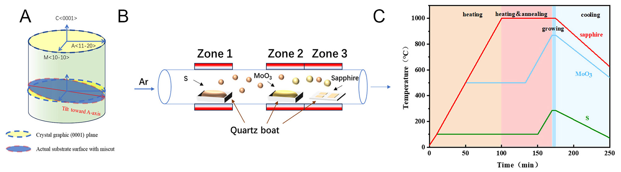
Figure 1. (A) Schematic illustration of the miscut of the sapphire wafer from an ingot. (B) Schematic diagram of the CVD system for MoS2 synthesis. (C) Schematic diagrams of the growth temperature ramps.
Fabrication of MoS2-based TENG
The synthesized MoS2/sapphire is fixed on an acrylic plate (20 mm × 30 mm × 0.1 mm). After an Ag electrode has been plated on the substrate by a coating machine, the liquid metal is spin-coated onto the Ag tape and affixed on top of the plated Ag electrode. Subsequently expanded polytetrafluoroethylene (E-PTFE) is covered over the Ag electrodes and seamlessly connected to the substrate, connecting the two ends of the Ag electrodes to form a closed circuit.
Characterizations and measurements
Optical microscopy (OM, Nikon LV100), scanning electron microscopy (SEM, ZEISS Gemini Sigma 300), and atomic force microscopy (AFM, Bruker Dimension Icon) probes adopt the contact mode, and the test area is the boundary between MoS2 grains and the substrate. The height difference between MoS2 and the substrate was measured by NanoScope Analysis software. The MoS2 grains were tested by X-ray photoelectron spectroscopy analysis (XPS, Thermo Fisher Scientific K-Alpha), and the C 1s peak (284.8 eV) was employed as a reference for calibration. Raman spectroscopy (HORIBA JY LabRAM HR Evolution with 532 nm laser) was used to characterize the synthesized MoS2. Polarized second-harmonic generation (SHG) microscopy measurements were performed in a homemade system. A femtosecond laser with 780 nm central wavelength (~100 fs, 100 MHz, generated by MenloSystems) and power of 1.8 mW was used to excite the sample. The laser beam passed through a linear polarizer and was tightly focused to ~1 µm spot diameter by a 100× objective (NA = 0.9, Nikon). The MoS2 samples were attached to a piezoelectric stage to realize sub-micrometer scanning. Analog-to-digital conversion (ADC) collection system (Keithley 6514) was used to measure the charge, voltage and current.
RESULTS AND DISCUSSION
Growth mechanism of aligned MoS2
When the substrate symmetry is a subset of the 2D material, the 2D material has fewer low-energy orientations on the substrate[36]. As shown in Figure 2A, MoS2 with threefold symmetry has two low-energy orientations on a two- or six-fold symmetry substrate, and four low-energy orientations on a four-fold symmetry substrate. Two strategies have been identified for the growth of aligned MoS2: (1) Direct growth is achieved by exploiting the symmetry of MoS2 and the substrate. When the symmetry of the substrate lattice is matched with that of MoS2, MoS2 is able to achieve less orientation variant growth. This strategy typically necessitates the assistance of hydrogen or oxygen during the growth process[37] and it is incompatible with the single orientation growth of MoS2; (2) Substrate pretreatment. Steps are formed by annealing, lithography, and etching of the substrate[38]. The MoS2 edges have higher binding energy at the edges of the steps, thus realizing the aligned growth.
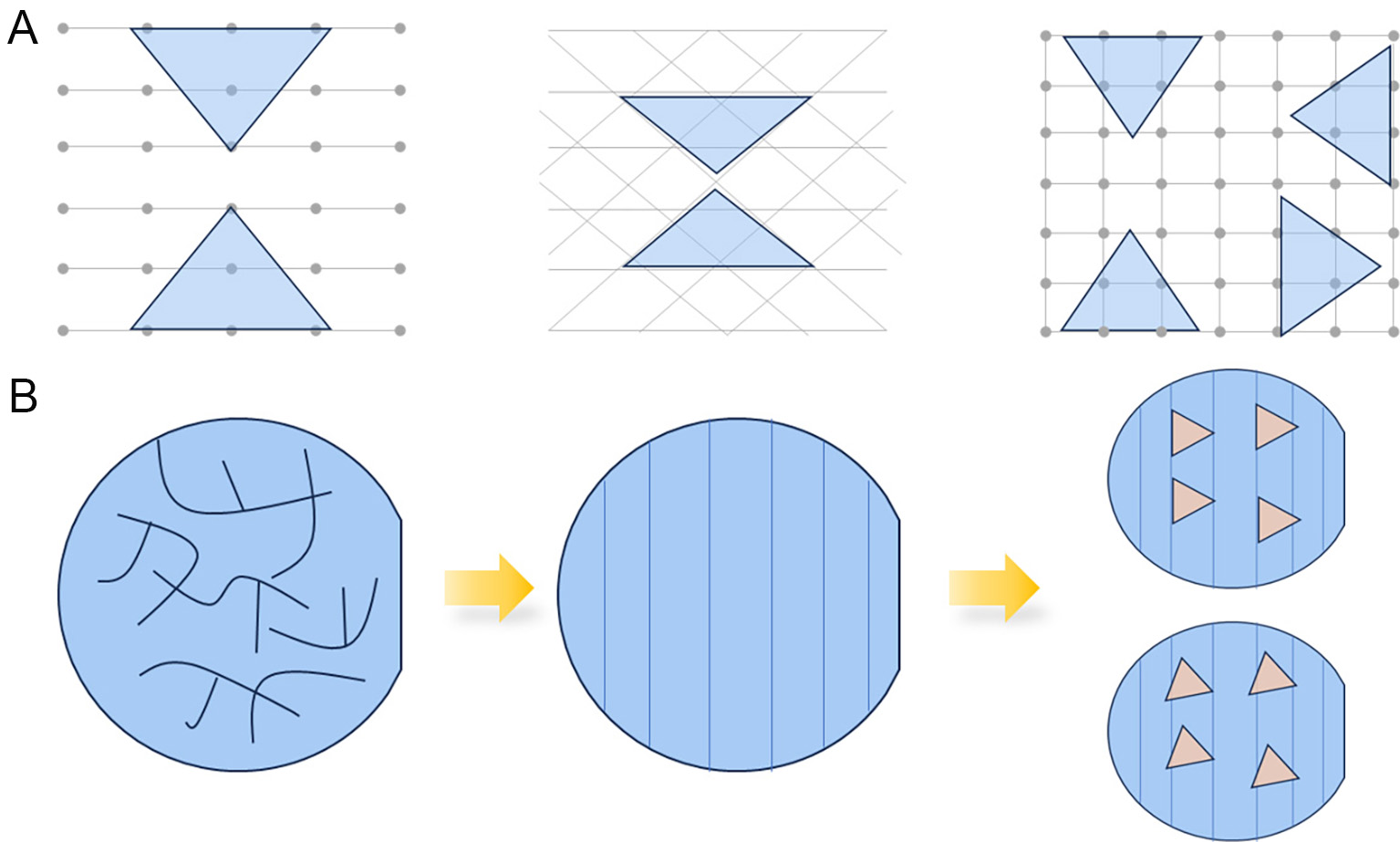
Figure 2. (A) Schematic illustration of a threefold symmetric 2D material on a two-, six-, and four-fold symmetric substrate, respectively. (B) Schematic illustration of the sapphire parallel steps formation and MoS2 growth process.
In this process, the pretreatment of the substrate is employed to create steps on the sapphire through annealing. As shown in Figure 2B, the initial sapphire surface is disordered, and parallel steps appear on the sapphire surface after annealing. These steps promote MoS2 aligned growth. Figure 3A and B shows the AFM image of sapphire without and with annealing treatment. Figure 3C corresponds to the height profile of the red line in Figure 3B and D shows the OM image of the CVD deposited aligned MoS2. The results indicate that the height of the steps is approximately 200 pm. Ultimately, the MoS2 grains exhibit alignment growth.
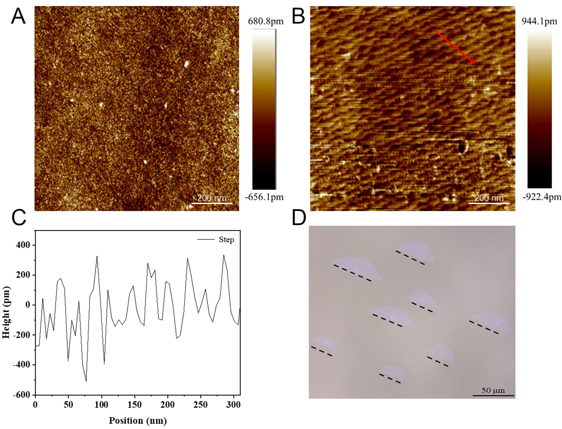
Figure 3. (A) AFM image of sapphire before annealing. (B) AFM image of sapphire after annealing. The height profile (C) is along the red lines in (B). (D) OM image of the CVD deposited aligned MoS2.
One-step preparation of aligned MoS2
The conventional methods for the preparation of aligned MoS2 typically necessitate prolonged annealing in air or oxygen atmosphere[39,40]. The substrate must await the cooling of the temperature zone after the annealing period of one to four hours before commencing the substrate next growth process, and the total duration of the annealing step exceeds 8 h. This approach is exceedingly time-consuming and energy-consuming. Meanwhile, it significantly increases the preparation cost.
Here, we observe that the short annealing time is sufficient to form steps on the substrate. When the steps are formed, the initial nucleated MoS2 grains tend to preferentially deposit at the edge of the step. The precursor is directly transported from the low-temperature zone of the CVD to the third temperature zone, where it can be directly deposited to form aligned MoS2 without cooling in the annealing temperature zone. This method simplifies the preparation steps of MoS2, thereby reducing the preparation time and cost. As shown in Figure 4, we compare the samples produced by no miscut sapphire [Figure 4A], unannealed sapphire [Figure 4B], and annealed sapphire at 850 °C [Figure 4C] with the samples prepared by the one-step method [Figure 4D]. Samples without miscut sapphire have inferior morphology and are difficult to discriminate between the orientations. In addition, the MoS2 grown from without miscut sapphire is prone to stacking in banded patterns. Samples of unannealed sapphire exhibit random orientations due to the absence of step formation. Because the growth temperature is 1,000 °C, its grain size reaches 100 µm. The smaller grain size of the 850 °C anneal compared to the 1,000 °C anneal is due to the fact that the high temperature of 1,000 °C makes the precursor gases more active and more evenly distributed on the substrate. Meanwhile, at 850 °C, no steps can be formed on the substrate, so the grains show random orientation.
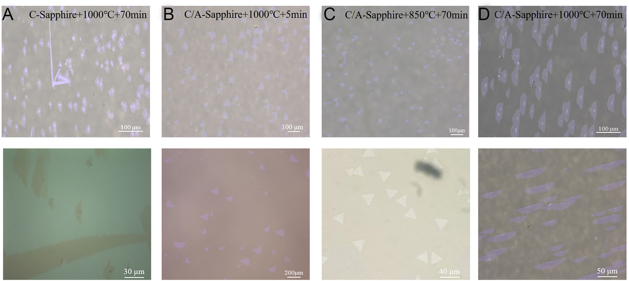
Figure 4. OM image of MoS2 growing under different parameters.
In particular, 3 mg of molybdenum oxide is required for the sample at 850 °C, and only 0.5 mg is required for annealing at 1,000 °C. This is due to the fact that the temperature of the third zone is 1,000 °C and the temperature of the second zone is 850 °C. According to the P V = n k T equation, there is a pressure difference between the third zone and the second zone[22,41], and the precursor gases tend to diffuse into the second zone and remain in the tube furnace for a longer period of time. Therefore, this method simplifies the preparation steps of MoS2, reduces the preparation time and raw material costs, and is conducive to grain size increase and uniformity.
Characterization of aligned MoS2
Figure 5A and B depicts the OM and SEM images of the prepared aligned MoS2. From Figure 5A and B, it can be seen that the MoS2 grains grow in the same direction, and the grain sizes range from 80 to 200 µm. The majority of MoS2 grains exhibit a trapezoidal morphology, which is attributed to the high growth temperature. The insulation of the sapphire substrate impairs the clarity of the SEM image, preventing the determination of whether secondary growth occurs on the grain surface. It is evident that the MoS2 has larger grain sizes and exhibits directional growth.
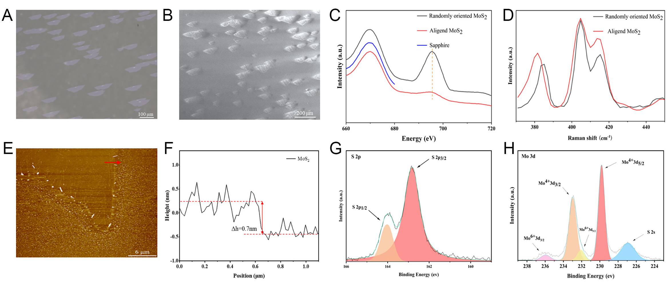
Figure 5. (A) OM image of the CVD deposited aligned MoS2. (B) SEM image of the CVD deposited aligned MoS2. (C) PL spectra of aligned MoS2 (red line) and randomly oriented MoS2 (black line). (D) Raman spectra of aligned MoS2 (red line) and randomly oriented MoS2 (black line). (E) AFM image of the MoS2 flake. The height profile (F) is along the red lines in (E). XPS spectra of (G) S 2p and (H) Mo 3d.
The photoluminescence (PL) spectra of the aligned MoS2 and randomly oriented MoS2 were obtained, as illustrated in Figure 5C. The aligned MoS2 exhibited a notable quenching in PL intensity compared to the randomly oriented MoS2, which was due to the strong coupling of the aligned MoS2 with the substrate. To further investigate the strong coupling between aligned MoS2 and the substrate, Raman spectroscopy tests were performed on aligned MoS2 and randomly oriented MoS2. As illustrated in Figure 5D, the rightmost peak is the sapphire substrate characteristic peak. We use the sapphire characteristic peak as a benchmark to compare the E2g peak positions of the two MoS2 samples. The E2g peak position of randomly oriented MoS2 is located at 385.1 cm-1, while the E2g peak position of aligned MoS2 is noted at 381.6 cm-1. The E2g peak of aligned MoS2 shows a red shift, demonstrating strong coupling between aligned MoS2 and the substrate with tensile strain[42,43]. Annealing appears to have enhanced the epilayer-substrate bonding. In order to initially characterize the thickness of aligned MoS2, the frequency difference between the peak positions of aligned MoS2 E2g and A1g was calculated to be 22 cm-1, which suggests MoS2 to be around one monolayer thick[44,45].
The thickness of the aligned MoS2 was accurately characterized by AFM, as illustrated in Figure 5E. Figure 5F depicts the height profile corresponding to the red line in Figure 5E. The aligned MoS2 exhibits a thickness of approximately 0.7 nm, which is consistent with that of monolayer MoS2 (0.65 nm).
To analyze the binding energy of the Mo and S atoms in the aligned MoS2, XPS was performed. The C 1s peak (284.8 eV) was employed as a reference for calibration. The S 2p spectrum [Figure 5G] exhibits two characteristic peaks at 162.8 and 164 eV, which correspond to the S 2p1/2 and S 2p3/2 orbitals, respectively. The Mo 3d spectrum [Figure 5H] exhibits characteristic peaks at 236.1, 233.1, 232.1, 230, and 227.2 eV, which correspond to the Mo6+ 3d3/2, Mo4+ 3d3/2, Mo6+ 3d5/2, Mo4+ 3d5/2 and S 2s orbitals, respectively. The characteristic peaks are consistent with previous reports[46-48], indicating that the prepared sample has a relatively pure MoS2 phase.
To ascertain the growth orientation degree of the MoS2 grains, we selected six different sites [Figure 6A] on the same substrate for observation and analysis. Figure 6B-G depicts the OM images of the six locations. From Figure 4, it can be seen that most of the grain sizes are over 100 µm. The orientation of 233 grains on the substrate was counted using the image j software with the horizontal orientation as a reference. The schematic diagram is shown in the upper right corner of Figure 6H. As shown in Figure 6H, the grain orientation is mainly distributed in the range of 11°-16°, and 73.8% grains are distributed in the range of 12°-15°. This proves that the orientation rate of our prepared samples exceeds 70%.
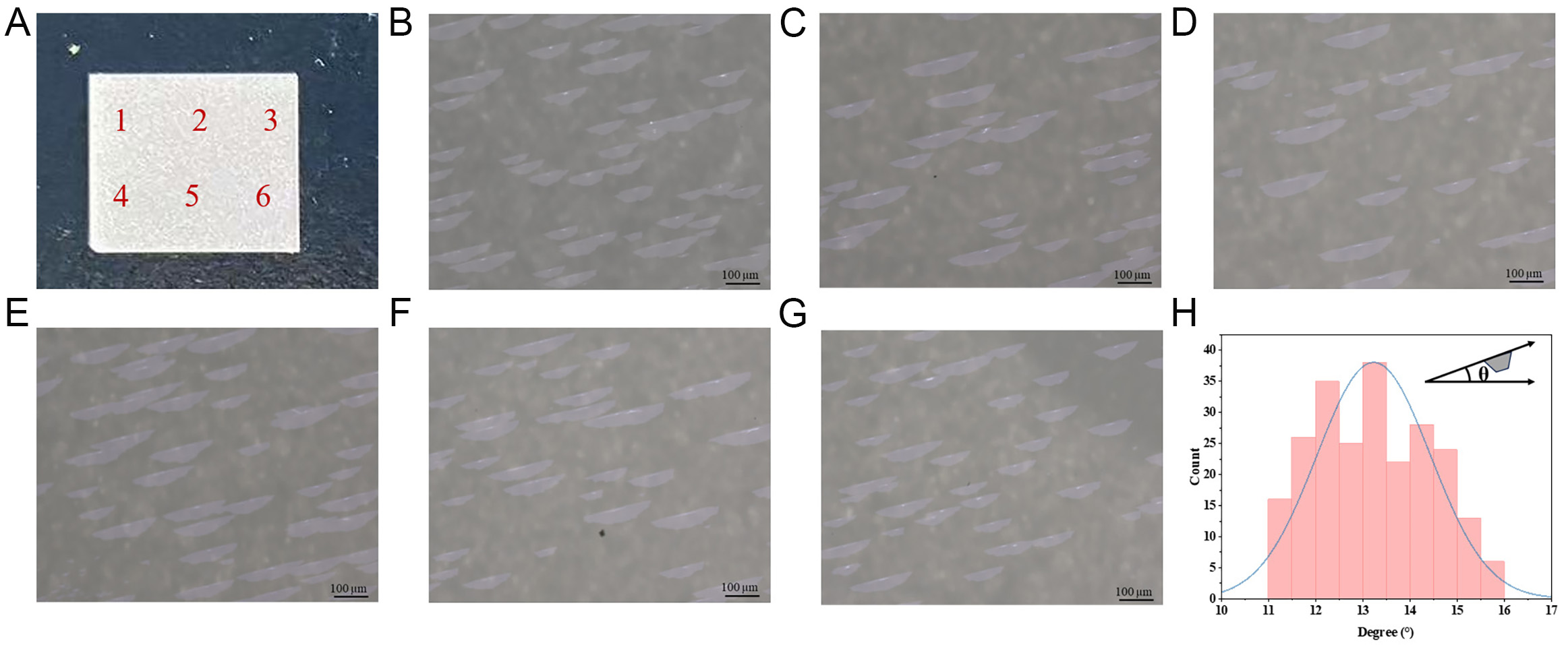
Figure 6. OM images for six positions on the sapphire, (B-G) correspond to 1-6 in (A). (H) Statistical distribution of MoS2 domains.
To explore their lattice orientations and grain boundaries at merging, Polarized SHG characterizations were performed. Figure 7A shows the OM image of MoS2 grains combined. Figure 7B demonstrates the SHG mapping image of the red region in Figure 7A. There is no decrease in intensity in the merged grains, indicating that no grain boundaries exist[38]. Figure 7C-F presents the five polarization resolved SHG patterns across a 1 cm2 sample area. The nearly overlapped SHG six-petal patterns confirm the coherent lattice orientation and uniformity of the as-grown MoS2 nanosheet[33].
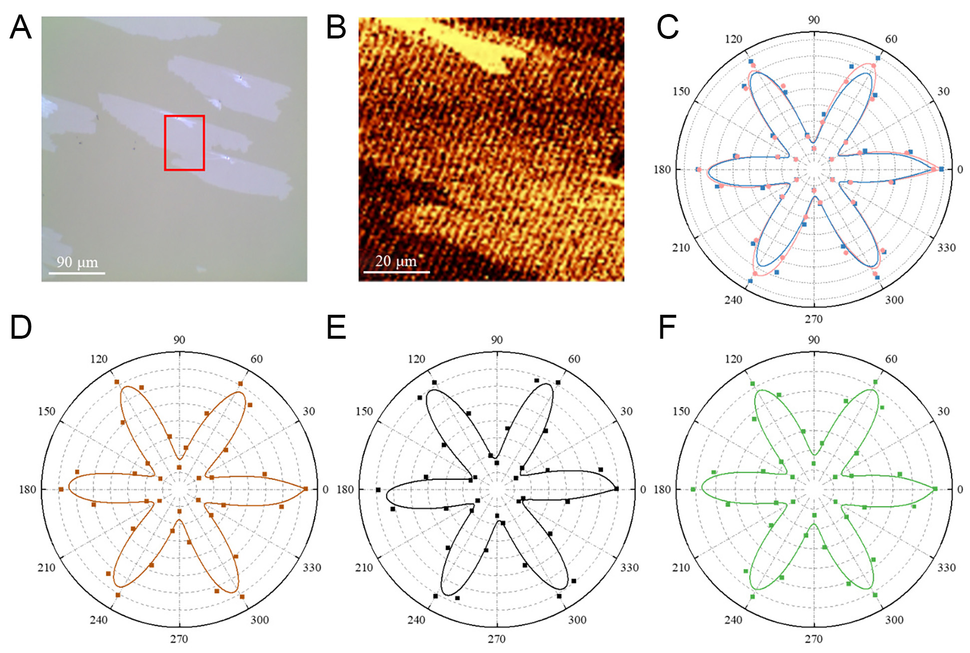
Figure 7. (A) OM image of two merging MoS2 domains. (B) SHG mapping of two merging MoS2 domains in the red region in (A). (C-F) Polar plot (°) of the SHG intensity of five MoS2 grains on the same substrate.
Electrical performance testing of MoS2-based TENG
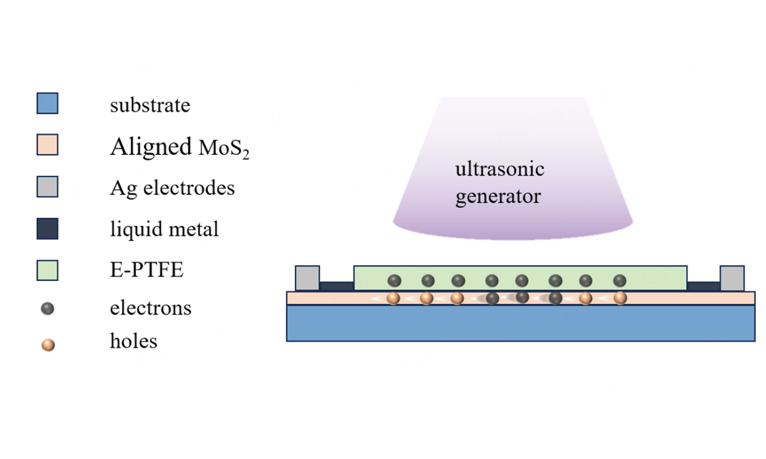
The charge transfer characteristics at the interface between MoS2 and E-PTFE were studied using TENG as a charge transfer probe and ultrasound as an energy source. The Ag electrode was evaporated on MoS2 using the coater and mask, as illustrated in Figure 8A. Fix the sapphire after evaporating the electrode onto an acrylic plate (The MoS2-based TENG photo is shown in Supplementary Figure 2). Due to the inability to directly connect the vaporized silver electrode to the alligator clips, the subsequent step involves spin-coating liquid metal onto silver tape. Attach the silver tape to the E-PTFE surface according to the width of the evaporated electrode and affix it on top of the vaporized Ag electrode. The particle size of the vaporized Ag electrode is small, and the direct adhesion of the Ag tape is not able to maintain the conduction. Spin-coating the liquid metal can improve the conduction ability of the Ag tape with the vaporized Ag electrode. In conclusion, the device is composed of MoS2 on the bottom, vaporized Ag electrode, liquid metallic Ag tape, and E-PTFE on the top surface [Figure 8B].
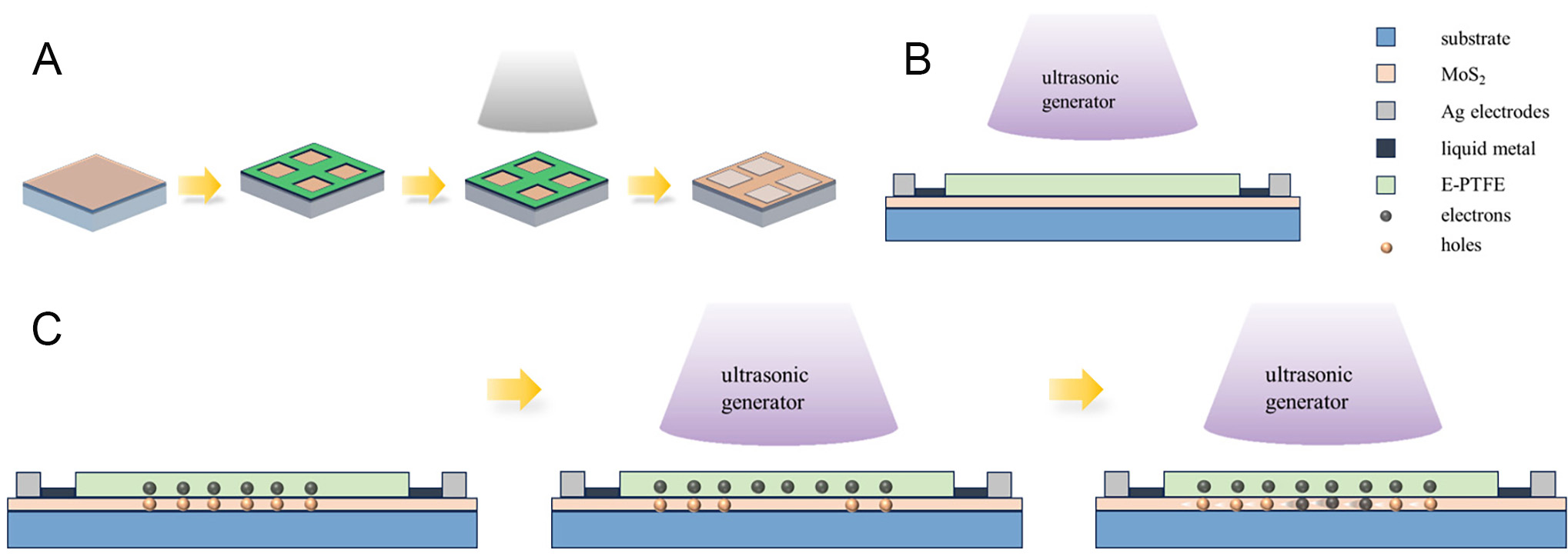
Figure 8. (A) Schematic diagram of silver electrode vaporization. (B) Schematic structure of MoS2-based TENG. (C) Working mechanism of the MoS2-based TENG.
In order to gain a deeper understanding of the operation principle of MoS2-based TENG devices, the fundamental principle of charge generation and transfer between the MoS2-PTFE layers during the operation of the ultrasonic generator is studied. As illustrated in Figure 8C, E-PTFE is electronegative. When MoS2 and E-PTFE come into contact with each other, the electric-double layer is formed at the interface between the MoS2 and E-PTFE. This is in equilibrium and there is no charge movement[17]. When ultrasonic waves are applied to the device surface, more negative charges accumulate on the E-PTFE surface and more holes appear on the corresponding MoS2 surface. In order to establish electrostatic equilibrium, the electrons on the MoS2 surface move in a directional manner to fill the holes, which are ultimately collected by the TENG probes.
The voltage, current, and charge generated by the MoS2-based TENG under ultrasonic waves are studied. As illustrated in Figure 9A-C, when the ultrasonic generator is turned on and off, it is possible to observe the rise and fall of the voltage, current, and charge generated between the Ag electrodes at both ends. After the ultrasonic generator is stopped, both voltage and current cease to exist, and the accumulated charge is diminished. It is noteworthy that the MoS2-based TENG can generate a voltage exceeding 120 V, a current of 1 mA, and accumulate a charge of 1,200 nC within a brief interval. From the area of the device (1 cm2), a current density of 10 A/m2 is obtained, indicating that the aligned MoS2 has excellent charge transport performance.
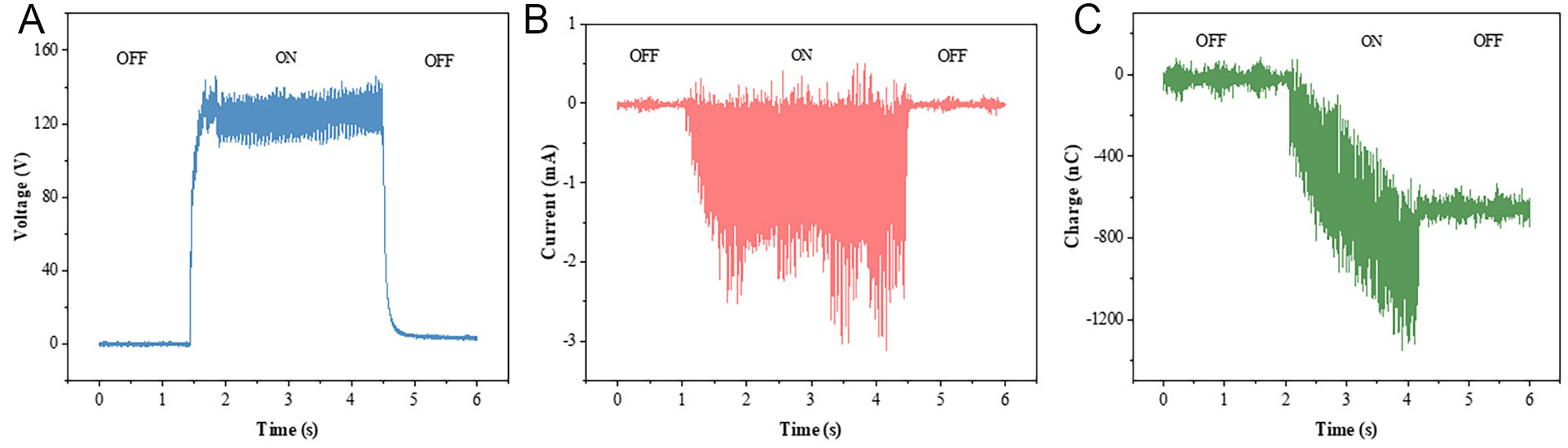
Figure 9. MoS2-based TENG voltage (A), current (B), and charge (C) in the ultrasonic on-off state.
In order to investigate the effect of ultrasonic power on charge transfer, we measured the voltage, current and charge of the electrodes at both ends of the device for 5 s at 10-50 W power, respectively. As illustrated in Figure 10A-C, the current voltage magnitude and charge accumulation rate of the MoS2-based TENG increase with the increase of the ultrasonic power. Ultrasonic waves accelerate the charge movement in the MoS2-PTFE electric double layer. In particular, the rise in charge accumulation within 5 s at both power levels (40-50 W) is not substantial due to the limitation of the device size on the total charge, and then the charge accumulation reaches its peak.
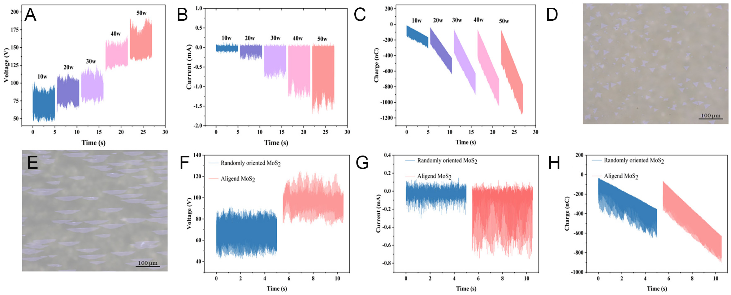
Figure 10. Aligned MoS2-based TENG voltage (A), current (B), and charge (C) at different ultrasonic powers. Optical microscope image of randomly oriented MoS2 (D) and aligned MoS2 (E). Randomly oriented and aligned MoS2-based TENG voltage (F), current (G), and charge (H).
In order to investigate the electrical properties of randomly oriented MoS2 and aligned MoS2, we measure the device electrical signals by using two kinds of them as charge transport layers, respectively. The OM images of randomly oriented MoS2 and aligned MoS2 are shown in Figure 10D and E, respectively. As shown in Figure 10F-H, we select the voltage, current, and charge signals output from the device within 5 s for comparison while keeping other parameters consistent. The aligned MoS2 device was able to output a voltage of 120 V, a peak current of 0.7 mA, and accumulate a charge of 900 nC under the same test conditions, whereas the randomly oriented MoS2 device could only output a voltage of 85 V, a peak current of 0.2 mA, and an accumulated charge of 600 nC. The results of the superiority of aligned MoS2 devices over randomly oriented MoS2 devices can be demonstrated by the fact that grain boundaries and defects at the merging of randomly oriented MoS2 grains lead to the compounding of a large number of electrons and holes during the charge transport process, which affects the transport of carriers. The MoS2-based TENG generates high voltage, current, and accumulated charge under the influence of ultrasonic waves. Consequently, the aligned MoS2 is regarded as a promising candidate for charge transfer.
CONCLUSIONS
In conclusion, a one-step deposition strategy was employed to prepare highly aligned MoS2 nanosheets. Through the detailed characterization of MoS2 nanosheets, it was observed that they have large dimensions and orientation rate of over 70%, which enables us to prepare aligned MoS2 nanosheets at a low cost in a short period of time. Meanwhile, we employed a TENG as a charge transfer test probe to evaluate the charge transfer capability of aligned MoS2 nanosheets under different ultrasonic powers. The aligned MoS2 nanosheets exhibit high voltage, current, and charge under ultrasonic waves. The charge transport properties of randomly oriented and aligned MoS2 were compared by TENG. Furthermore, compared with the conventional low-frequency mechanical work, choosing high-frequency ultrasound as the energy source broadens the scope application of aligned MoS2 in the TENG field. This indicates that the aligned MoS2 nanosheet exhibits considerable potential in charge transfer and energy harvesting applications.
DECLARATIONS
Author Contributions
Data curation, methodology, writing - original draft: Li, J.
Data curation, investigation: Guo, J.
Writing - review & editing: Zhang, Y.
Investigation: Zhang, A.
Formal analysis, project administration: Yang, W.
Formal analysis, resources: Feng, X.
Data curation, validation: Zhang, Y.
Funding acquisition, project administration: Yang, P.
Availability of data and materials
The detailed materials and methods in the experiment are available within the manuscript. Further data are available from the corresponding author upon reasonable request.
Financial support and sponsorship
This work was financially supported by the Yunnan Provincial Science and Technology Project at Southwest United Graduate School (202302A0370009), the National Natural Science Foundation of China (Nos. 12264057, 52202312), the Key Applied Basic Research Program of Yunnan Province (202201AS070023), Project for Building a Science and Technology Innovation Center Facing South Asia and Southeast Asia (202403AP140015), Yunnan Revitalization Talent Support Program, the Spring City Plan: The High-level Talent Promotion and Training Project of Kunming (2022SCP005), and the Science Foundation of the Chinese Academy of Sciences.
Conflicts of interest
All authors declared that there are no conflicts of interest.
Ethical approval and consent to participate
Not applicable.
Consent for publication
Not applicable.
Copyright
© The Author(s) 2025.
Supplementary Materials
REFERENCES
1. Zhang, Z.; Yang, X.; Liu, K.; Wang, R. Epitaxy of 2D materials toward single crystals. Adv. Sci. 2022, 9, e2105201.
2. Yang, M.; Xiong, K.; Chen, X.; Zhong, H.; Lin, S. Ultra-low-power-consuming liquid-water-based optoelectronic computing chip. Device 2024, 2, 100547.
3. Cheng, Z.; Cao, R.; Wei, K.; et al. 2D materials enabled next-generation integrated optoelectronics: from fabrication to applications. Adv. Sci. 2021, 8, e2003834.
4. Splendiani, A.; Sun, L.; Zhang, Y.; et al. Emerging photoluminescence in monolayer MoS2. Nano. Lett. 2010, 10, 1271-5.
5. Mak, K. F.; Lee, C.; Hone, J.; Shan, J.; Heinz, T. F. Atomically thin MoS2: a new direct-gap semiconductor. Phys. Rev. Lett. 2010, 105, 136805.
6. Zhang, X.; Nan, H.; Xiao, S.; et al. Shape-uniform, high-quality monolayered MoS2 crystals for gate-tunable photoluminescence. ACS. Appl. Mater. Interfaces. 2017, 9, 42121-30.
7. Liu, H.; Si, M.; Najmaei, S.; et al. Statistical study of deep submicron dual-gated field-effect transistors on monolayer chemical vapor deposition molybdenum disulfide films. Nano. Lett. 2013, 13, 2640-6.
8. Kang, M.; Kim, S. J.; Song, W.; et al. Fabrication of flexible optoelectronic devices based on MoS2/graphene hybrid patterns by a soft lithographic patterning method. Carbon 2017, 116, 167-73.
9. Gautam, S.; Chugh, S.; Gates, B. D. Electrodeposition of PdPt nanoparticles on edges and S-vacancies in exfoliated MoS2 nanosheets for enhanced hydrogen evolution activity. ChemSusChem 2024, 17, e202301922.
10. Gao, Q.; Zhang, C.; Yang, K.; et al. High-performance CVD bilayer MoS2 radio frequency transistors and gigahertz mixers for flexible nanoelectronics. Micromachines 2021, 12, 451.
11. Kim, J. K.; Song, Y.; Kim, T. Y.; et al. Analysis of noise generation and electric conduction at grain boundaries in CVD-grown MoS2 field effect transistors. Nanotechnology 2017, 28, 47LT01.
12. Khandelwal, G.; Deswal, S.; Shakthivel, D.; Dahiya, R. Recent developments in 2D materials for energy harvesting applications. J. Phys. Energy. 2023, 5, 032001.
13. Priya, S.; Mandal, D.; Chowdhury, A.; Kansal, S.; Chandra, A. Time-dependent exfoliation study of MoS2 for its use as a cathode material in high-performance hybrid supercapacitors. Nanoscale. Adv. 2023, 5, 1172-82.
14. Singh, A.; Mishra, A. K. Large area CVD-grown vertically and horizontally oriented MoS2 nanostructures as SERS biosensors for single molecule detection. Nanoscale 2023, 15, 16480-92.
15. Xu, C.; Pan, C.; Liu, Y.; Wang, Z. Hybrid cells for simultaneously harvesting multi-type energies for self-powered micro/nanosystems. Nano. Energy. 2012, 1, 259-72.
16. Oh, H.; Kwak, S. S.; Kim, B.; et al. Highly conductive ferroelectric cellulose composite papers for efficient triboelectric nanogenerators. Adv. Funct. Mater. 2019, 29, 1904066.
17. Ye, X.; Zheng, Z.; Werner, J. G.; Boley, J. W. Mechanically rupturing liquid metal oxide induces electrochemical energy (Adv. Funct. Mater. 31/2024). Adv. Funct. Mater. 2024, 34, 2470174.
18. Yang, C.; He, J.; Guo, Y.; et al. Highly conductive liquid metal electrode based stretchable piezoelectric-enhanced triboelectric nanogenerator for harvesting irregular mechanical energy. Mater. Des. 2021, 201, 109508.
19. Ahmadi, R.; Abnavi, A.; Hasani, A.; et al. Pseudocapacitance-induced synaptic plasticity of tribo-phototronic effect between ionic liquid and 2D MoS2. Small 2024, 20, e2304988.
20. Aji, A. S.; Nishi, R.; Ago, H.; Ohno, Y. High output voltage generation of over 5 V from liquid motion on single-layer MoS2. Nano. Energy. 2020, 68, 104370.
21. Kumar, S.; Sharma, A.; Gupta, V.; Tomar, M. Development of novel MoS2 hydrovoltaic nanogenerators for electricity generation from moving NaCl droplet. J. Alloys. Compd. 2021, 884, 161058.
22. Wang, T.; Guo, J.; Zhang, Y.; et al. Synthesis of high-quality monolayer MoS2 via a CVD upstream deposition strategy for charge capture and collection. Cryst. Growth. Des. 2024, 24, 2755-63.
23. van, der. Zande. A. M.; Huang, P. Y.; Chenet, D. A.; et al. Grains and grain boundaries in highly crystalline monolayer molybdenum disulphide. Nat. Mater. 2013, 12, 554-61.
24. You, J.; Hossain, M. D.; Luo, Z. Synthesis of 2D transition metal dichalcogenides by chemical vapor deposition with controlled layer number and morphology. Nano. Converg. 2018, 5, 26.
25. Zhao, T.; Guo, J.; Li, T.; et al. Substrate engineering for wafer-scale two-dimensional material growth: strategies, mechanisms, and perspectives. Chem. Soc. Rev. 2023, 52, 1650-71.
26. Chen, L.; Liu, B.; Ge, M.; Ma, Y.; Abbas, A. N.; Zhou, C. Step-edge-guided nucleation and growth of aligned WSe2 on sapphire via a layer-over-layer growth mode. ACS. Nano. 2015, 9, 8368-75.
27. Yu, H.; Yang, Z.; Du, L.; et al. Precisely aligned monolayer MoS2 epitaxially grown on h-BN basal plane. Small 2017, 13, 1603005.
28. Zhou, X.; Xue, X.; Cai, L.; Liu, S.; Liu, M.; Yu, G. Large-area orientation-controlled growth of hexagonal boron nitride on liquid copper. ACS. Appl. Electron. Mater. 2022, 4, 6261-8.
29. Aljarb, A.; Cao, Z.; Tang, H. L.; et al. Substrate lattice-guided seed formation controls the orientation of 2D transition-metal dichalcogenides. ACS. Nano. 2017, 11, 9215-22.
30. Ji, Q.; Kan, M.; Zhang, Y.; et al. Unravelling orientation distribution and merging behavior of monolayer MoS2 domains on sapphire. Nano. Lett. 2015, 15, 198-205.
31. Park, Y.; Ahn, C.; Ahn, J. G.; et al. Critical role of surface termination of sapphire substrates in crystallographic epitaxial growth of MoS2 using inorganic molecular precursors. ACS. Nano. 2023, 17, 1196-205.
32. Liu, L.; Li, T.; Ma, L.; et al. Uniform nucleation and epitaxy of bilayer molybdenum disulfide on sapphire. Nature 2022, 605, 69-75.
33. Li, T.; Guo, W.; Ma, L.; et al. Epitaxial growth of wafer-scale molybdenum disulfide semiconductor single crystals on sapphire. Nat. Nanotechnol. 2021, 16, 1201-7.
34. Wang, Q.; Li, N.; Tang, J.; et al. Wafer-scale highly oriented monolayer MoS2 with large domain sizes. Nano. Lett. 2020, 20, 7193-9.
35. Ma, Z.; Wang, S.; Deng, Q.; et al. Epitaxial growth of rectangle shape MoS2 with highly aligned orientation on twofold symmetry a-Plane sapphire. Small 2020, 16, e2000596.
36. Dong, J.; Liu, Y.; Ding, F. Mechanisms of the epitaxial growth of two-dimensional polycrystals. NPJ. Comput. Mater. 2022, 8, 797.
37. Ji, H. G.; Lin, Y.; Nagashio, K.; et al. Hydrogen-assisted epitaxial growth of monolayer tungsten disulfide and seamless grain stitching. Chem. Mater. 2018, 30, 403-11.
38. Yao, W.; Wu, B.; Liu, Y. Growth and grain boundaries in 2D materials. ACS. Nano. 2020, 14, 9320-46.
39. Yang, P.; Liu, F.; Li, X.; et al. Highly reproducible epitaxial growth of wafer-scale single-crystal monolayer MoS2 on sapphire. Small. Methods. 2023, 7, e2300165.
40. Li, L.; Wang, Q.; Wu, F.; et al. Epitaxy of wafer-scale single-crystal MoS2 monolayer via buffer layer control. Nat. Commun. 2024, 15, 1825.
41. Rajan A, Warner JH, Blankschtein D, Strano MS. Generalized mechanistic model for the chemical vapor deposition of 2D transition metal dichalcogenide monolayers. ACS. Nano. 2016, 10, 4330-44.
42. Kang, L.; Tian, D.; Meng, L.; et al. Epitaxial growth of highly-aligned MoS2 on c-plane sapphire. Surf. Sci. 2022, 720, 122046.
43. Su, L.; Zhang, Y.; Yu, Y.; Cao, L. Dependence of coupling of quasi 2-D MoS2 with substrates on substrate types, probed by temperature dependent Raman scattering. Nanoscale 2014, 6, 4920-7.
44. Ling, X.; Lee, Y. H.; Lin, Y.; et al. Role of the seeding promoter in MoS2 growth by chemical vapor deposition. Nano. Lett. 2014, 14, 464-72.
45. Najmaei, S.; Liu, Z.; Zhou, W.; et al. Vapour phase growth and grain boundary structure of molybdenum disulphide atomic layers. Nat. Mater. 2013, 12, 754-9.
46. Li, J.; Wang, S.; Jiang, Q.; et al. Single-crystal MoS2 monolayer wafer grown on Au (111) film substrates. Small 2021, 17, e2100743.
47. Wu, S.; Zeng, Y.; Zeng, X.; et al. High-performance p-type MoS2 field-effect transistor by toroidal-magnetic-field controlled oxygen plasma doping. 2D. Mater. 2019, 6, 025007.
Cite This Article
How to Cite
Download Citation
Export Citation File:
Type of Import
Tips on Downloading Citation
Citation Manager File Format
Type of Import
Direct Import: When the Direct Import option is selected (the default state), a dialogue box will give you the option to Save or Open the downloaded citation data. Choosing Open will either launch your citation manager or give you a choice of applications with which to use the metadata. The Save option saves the file locally for later use.
Indirect Import: When the Indirect Import option is selected, the metadata is displayed and may be copied and pasted as needed.
About This Article
Copyright

Data & Comments
Data
0


Comments
Comments must be written in English. Spam, offensive content, impersonation, and private information will not be permitted. If any comment is reported and identified as inappropriate content by OAE staff, the comment will be removed without notice. If you have any queries or need any help, please contact us at [email protected].