


fig5
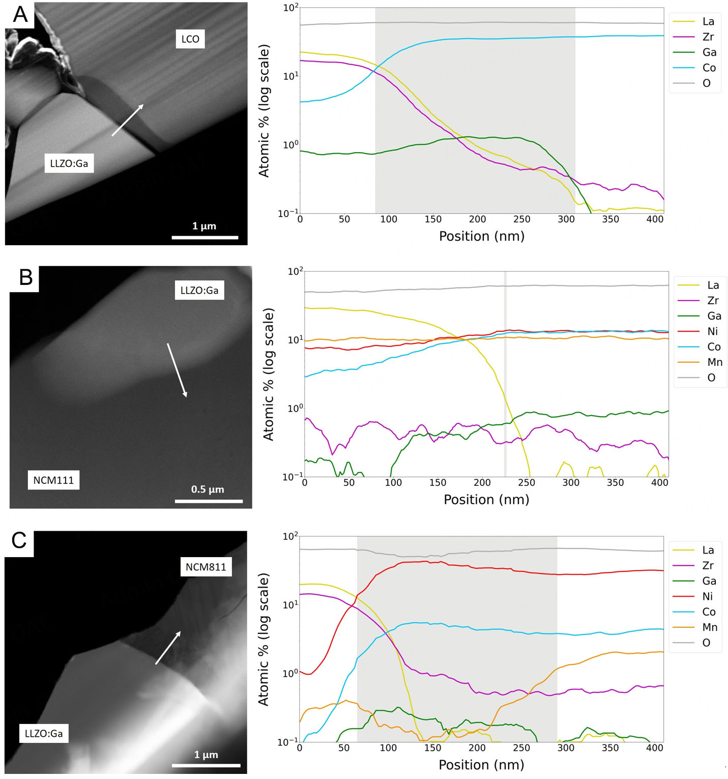
Figure 5. HAADF-STEM image (left) and EDS line scan (right) across the interface marked by the arrow for (A) LCO + LLZO:Ga, (B) NCM111 + LLZO:Ga, and (C) NCM811 + LLZO:Ga co-sintered at 1,000 °C. The light grey area in the EDS line scan represents the dark layer at the LCO/LLZO:Ga interface visible in the HAADF image. Further EDS mappings of these samples are available in the


