


fig5
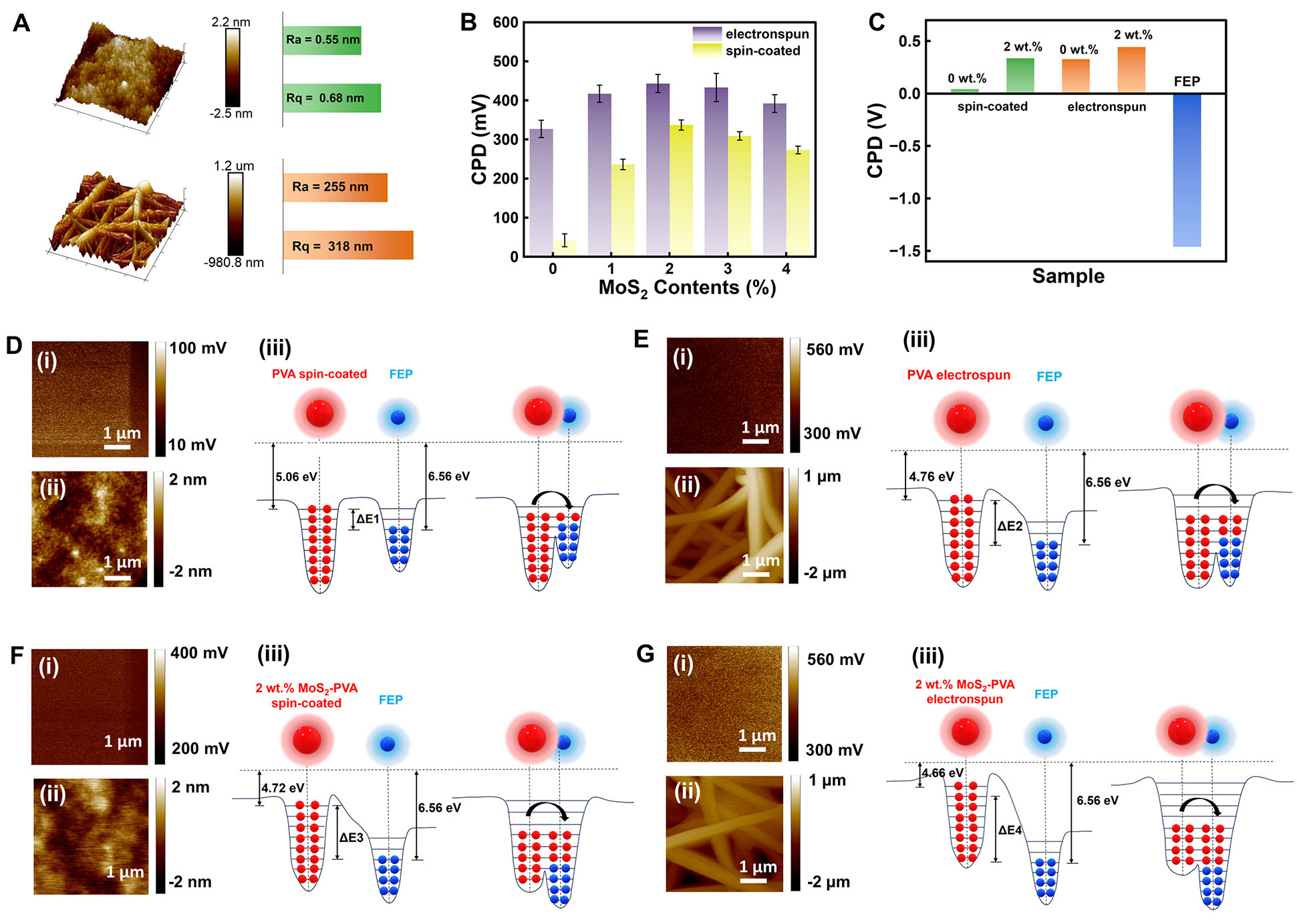
Figure 5. Surface morphology and surface potential analysis of pristine and MoS2-doped PVA films. (A) AFM images and corresponding roughness profiles of 2 wt.% MoS2-PVA spin-coated film (top) and 2 wt.% MoS2-PVA ES film (bottom). (B) CPD values extracted from KPFM for spin-coated and ES films. (C) Direct comparison of CPD values between pristine PVA, 2 wt.% MoS2-PVA films, and FEP. (D) KPFM results of pristine spin-coated PVA film: (i) potential energy profile, (ii) surface morphology, and (iii) schematic illustration of electron cloud distribution in the triboelectric pair before and after contact with FEP. (E) Corresponding results for pristine PVA ES film. (F) Corresponding results of 2 wt.% MoS2-PVA spin-coated film. (G) Corresponding results of 2 wt.% MoS2-PVA ES film.


