




Defects in CdTe single crystals for photon-counting imaging
 0
0 Abstract
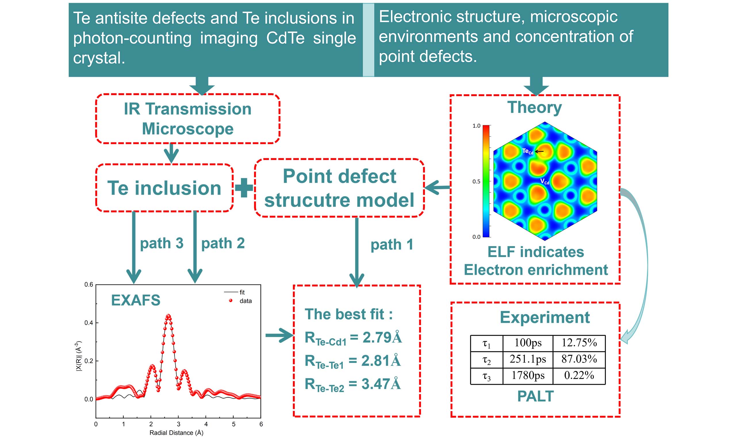
Photon counting imaging represents a revolutionary breakthrough, surpassing current scintillator-based imaging technology and holding significant promise for the field of medical computed tomography. CdTe is a representative example of a high-performance photon-counting imaging material. However, defects within it, particularly point defects, act as carrier trapping centers and are a key factor limiting its count rate capability. In this paper, the size distribution and density of Te inclusions in CdTe single crystal were first analyzed using an infrared transmission microscope. Subsequently, point defects were studied both theoretically and experimentally using modern research methods. Specifically, a point defect complex model was first established using the first-principles method based on density functional theory plus the Coulomb interaction potential (U). The calculated results show that electrons are localized around the point defect complex and its surrounding region, resulting in an increased electron density around it. This provides a theoretical basis for the reduced positron lifetime (100.0 ps) for the point defect states. Based on this value, the concentration of the defect complex was calculated to be
Keywords
INTRODUCTION
II-VI group semiconductors occupy a special place among functional materials, as their physical properties are largely determined by their crystal structure and structural defects. Therefore, the structural properties of these compounds must be studied precisely. In current clinical practice, X-ray computed tomography (CT) remains one of the most widely used techniques, where scintillation crystals serve as the primary imaging material[1,2]. However, a new class of II-VI semiconductors (known as photon-counting imaging materials) is emerging as a promising alternative by directly converting X-ray photons into electrical signals, thereby achieving significantly improved imaging resolution[3-5]. This category of materials includes cadmium telluride (CdTe), cadmium zinc telluride (CZT), and others, among which CdTe holds a leading position. The greatest challenge for CdTe materials in photon-counting imaging stems from the polarization effect induced by extremely high-dose X-ray irradiation[6,7]. Specifically, when the X-ray irradiation dose exceeds 107 counts/(mm2·s), the large quantities of charge carriers generated inside the CdTe detector cannot be collected promptly by the metal electrodes under the applied bias voltage. This leads to the accumulation of carriers, which introduces a built-in electric field and consequently degrades the detection efficiency, thereby affecting imaging quality. Research indicates that point defects in CdTe crystals act as carrier trapping centers, which is a key factor limiting their high-count-rate performance[8,9]. Trapping centers are generally associated with deep-level point defects inside the crystal. Luan et al. reported that the Te antisite (TeCd) acts as the dominant deep-level donor defect in CdTe crystals, impairing carrier mobility and lifetime via hole trapping[10]. Additionally, Guo et al. demonstrated that A-center defects associated with cadmium vacancies (VCd) act as key traps for holes, thereby leading to a significant reduction in both carrier lifetime and electron mobility[11]. Currently, the origin of deep-level point defects remains uncertain. Prominent among these are deep-level point defect complexes resulting from either deep-level doping or shallow-level doping[12]. Deep-level point defects can degrade material performance through two distinct mechanisms[13]. First, they trap carriers, which reduces carrier lifetime and prevents carriers from reaching the electrode. Second, when ionized, they create a Coulomb potential that scatters carriers, thereby reducing carrier mobility. Calculations show that when the Cl doping concentration increases from 1016 cm-3 to 1017 cm-3, the electron mobility decreases from 1,100 cm2/(V·s) to 650 cm2/(V·s), causing carriers to accumulate at the electrode and thereby reducing the time-resolved energy spectrum efficiency[14]. At the mesoscopic scale, if point defects form complexes such as [VCd-TeCd], their carrier capture cross-section can even be two orders of magnitude larger than that of monovacancies[15]. This causes the space charge density between electrodes to vary with the concentration of point defects, leading to a non-uniform electric field distribution within the detector. Under the influence of this non-uniform electric field distribution, the measured electric field intensity under a flux of 106 counts/(mm2·s) decreased by 40%[16]. Therefore, a thorough understanding of point defect behavior is key to improving the detection efficiency of CdTe crystals[17]. In addition, Te inclusions in CdTe are a major cause of detector performance degradation. These microscopic defects trap the free electrons generated by incident radiation, so entailing significant fluctuations in the total collected charge and thereby strongly affecting the energy resolution of thick (long-drift) detectors[18].
In this work, Te inclusions in CdTe were analyzed using IR transmission microscope. Furthermore, a combined theoretical and experimental approach was employed to investigate point defects in photon-counting-grade CdTe single crystals. First, density functional theory (DFT) with a Coulomb interaction potential (DFT + U) was used to accurately describe the electronic structure and local electron density of point defects. Second, X-ray photoelectron spectroscopy (XPS), positron annihilation spectroscopy (PAS), and X-ray absorption fine structure (XAFS) spectroscopy were employed to quantitatively analyze these point defects and to validate the theoretical findings.
MATERIALS AND METHODS
Crystal growth
The CdTe single crystal used in this study was grown via the melt growth technique, and the growth process, sample preparation and single crystal quality evaluation can be found in our previous study[10].
Theoretical calculation methods
This part of the study was performed using vienna ab initio software package (VASP). Based on our experimental results of point defect studies, a defect model incorporating Cd vacancies (VCd) and Te antisites (TeCd) was established using the method of the generalized gradient approximation with the Hubbard U correction (GGA + U), a Cd atom was selected at the coordinates (0, 0, 0) in a 2 × 2 × 2 supercell of the CdTe lattice, with another Cd atom placed at a distance d from it. By enumerating all possible relative positions of the two Cd atoms and considering periodic boundary conditions, five inequivalent structural models of point defects were obtained. Taking the lattice constant of the supercell a as the unit, the five models correspond to type H1 with d(1,1,0) = (
where pi is the probability of model i, kB is the Boltzmann constant, Ei is the energy of model i, E0 denotes the lowest energy among the five models, which corresponds to the H1, and T is the temperature. At 1,360 K, the typical growth temperature of CdTe single crystals, the models H1 to H5 have Boltzmann weights of 84.0%, 8.8%, 2.5%, 3.8%, and 0.8%, respectively. At room temperature, Boltzmann weight corresponding to H1 is ~99%. Therefore, the H1 model was selected in this study to represent the average level of the crystal defects, as it provides a reasonable approximation of the overall defect population.
All graphs in this section were generated using Origin software, except for the partial charge density and electron localization function plots, which were rendered using VESTA.
Experimental analysis methods
Te inclusions were observed using a Micronviewer 7290A infrared (IR) transmission microscope (Electrophysics, USA). Their sizes were measured and statistically analyzed using ImageJ software, and the size distribution graph was generated in Origin. XPS measurements were performed using a Shimadzu Kratos Axis Supra+ spectrometer (Shimadzu Corporation, Japan). XPS analysis was accomplished by irradiating a sample with monochromatic soft X-rays (Al Kα radiation) and then analyzing the binding energy of the emitted photoelectrons. Positron annihilation spectroscopy was carried out at room temperature using a US-made ORTEC DPLS3000 instrument (Ametek, USA). Positrons emitted from a 22Na source were incident upon the sample. Upon encountering defects during their diffusion, they become trapped in potential wells and subsequently annihilate with electrons. The rest mass of the positron is entirely converted into energy, typically released as two 511 keV gamma photons. These photons were detected using an EG&G ORTEC fast-fast coincidence system (Ametek, USA). This allows the free diffusion time of positrons in the sample to be determined, from which information such as the type and concentration of defects can be inferred. XAFS measurements were performed at the BL14W beamline of the Shanghai Synchrotron Radiation Facility (SSRF, Shanghai, China) using a Si (111) double-crystal monochromator. The spectra were collected at room temperature using a Bruker 5040 four-channel silicon drift detector (SDD). Both the Te K-edge X-ray absorption near edge structure (XANES) spectra and the extended X-ray absorption fine structure (EXAFS) spectra were recorded in transmission mode. The data were subsequently processed using the Athena and Artemis software for background subtraction, normalization, and data fitting. All figures in the experimental section were generated by Origin software.
RESULTS AND DISCUSSION
Analysis of Te inclusion by IR transmission microscope
Te inclusions are among the inevitable defects that degrade detector performance. Figure 1A is a composite of multiple IR transmission microscope images, showing the distribution of Te inclusions in CdTe single crystal.
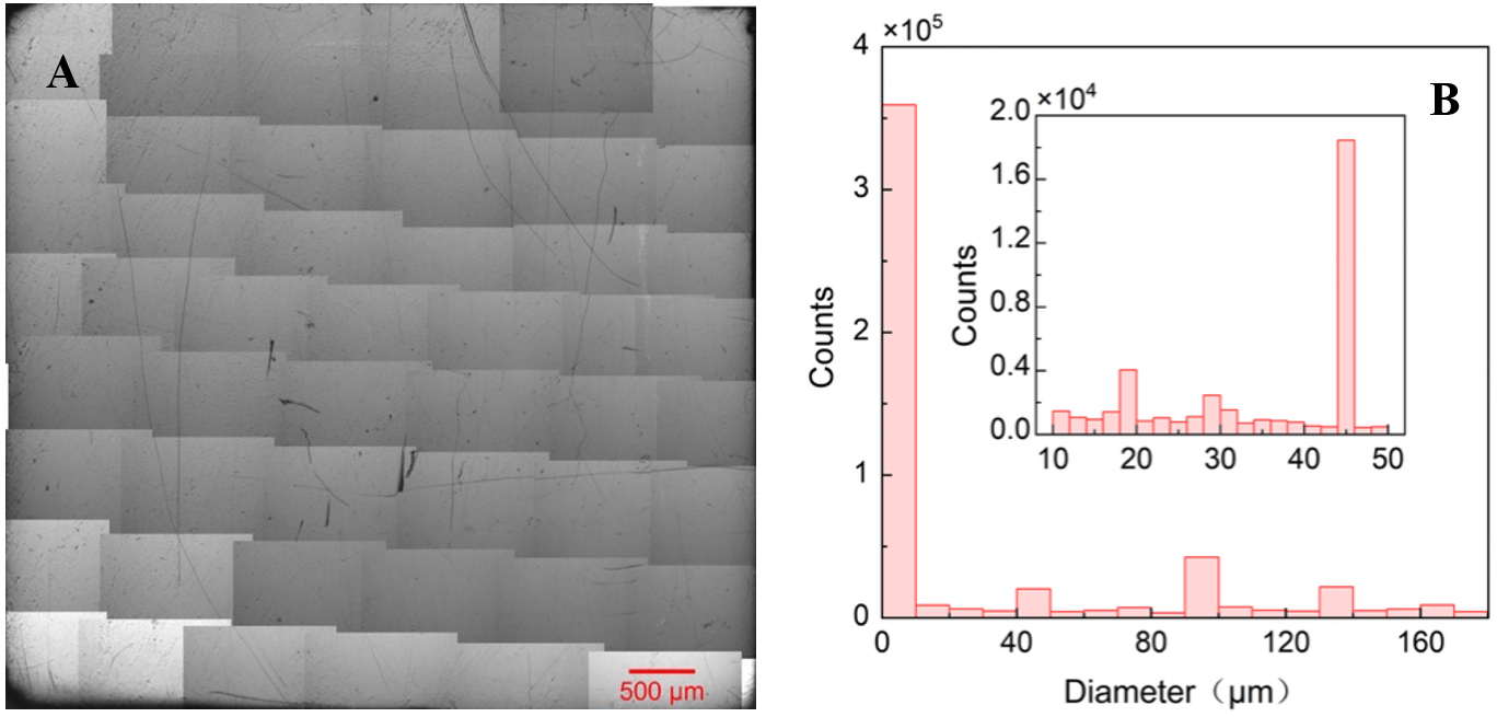
Figure 1. (A) Infrared transmission photographs of the CdTe single crystal, composited from multiple images, showing the distribution of Te inclusions over an area of approximately 5 × 5 mm2. (B) The corresponding dimensional statistics, where the size range of 0-10 µm accounts for the great majority. The inset shows a magnified view of the size distribution in the 10-50 μm range.
Figure 1B shows the size distribution. The results show that the great majority of Te inclusions fall within the size range of 0-10 μm and the density was around 2.108 × 104 cm-3. The inset shows the magnified view of the size distribution in the 10-50 μm range. This density in our crystal was slightly lower than that of CdTe grown by the traveling heater method (1 × 105 cm-3)[19] and CdTeSe grown by the high-pressure Bridgman method (7 × 104 cm-3)[20], and fell within the ranges in CdMnTe grown by the vertical Bridgman method [(2-8) × 104 cm-3][21]. During crystal growth, Cd evaporation causes the Te content in the melt to become nonuniform and enrich ahead of the solid-liquid interface, leading to local constitutional supercooling. This drives the growth interface to develop into a small cellular morphology[22]. As Te droplets approach the liquid-solid interface, they are engulfed by the faster-growing cells and ultimately precipitate as Te inclusions in the ingot. Bolotnikov et al. reported a correlation between defect concentration and device performance, showing that Te inclusions with diameters of < 3 μm do not affect charge transport, even at concentrations as high as 3 × 106 cm-3[23]. This indicates that the Te inclusions of our crystals have little impact on the charge transport performance of the detectors.
Simulations of electronic structure and electron density of point defects
A point defect model, as described in the theoretical calculation method section, is adopted here to accurately describe the electronic structure and electron density of the defects. It is worth noting that the high-precision structural optimization and static self-consistent calculations were initially conducted by employing Hubbard U corrections of UCd, d = 7.381 eV for the Cd d-orbitals and UTe, p = -7.912 eV for the Te p-orbitals[24]. The final structural parameters for the CdTe were converged to a bond length of 2.83201 Å, a bond angle of 109°28'32", and a primitive cell lattice constant of 6.54026 Å, all of which are in excellent agreement with the ab initio calculation values for bulk CdTe[25].
To analyze the electronic properties of point defects and their surroundings, the calculated density of states (DOS) result is shown in Figure 2, where Figure 2A presents the DOS of the defect-free crystal. It is shown that the valence band maximum (VBM) is dominated by Te-p orbitals, whereas the conduction band minimum (CBM) originates primarily from Cd-s and Te-p orbitals, with a band gap of Eg = 1.4256 eV. This calculated band gap agrees remarkably well with the experimental value[10]. Figure 2B displays DOS for the CdTe containing the [VCd-TeCd] complex. Evidently, additional energy levels emerge within the band gap, with E1 and E2 located at 0.6522 and 0.7112 eV above the VBM, respectively, while E3 is located at
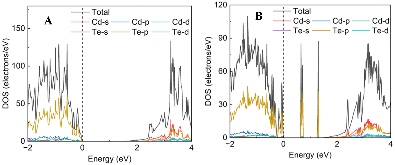
Figure 2. Density of states (DOS) diagram. (A) The defect-free CdTe lattice shows a band gap of 1.4256 eV. (B) The [VCd-TeCd] complex introduces the defect energy levels at 0.6522 eV(E1) and 0.7112 eV (E2) above the VBM and 0.1264 eV (E3) below the CBM, which are derived mainly by Te p and d orbitals.
From the DOS plot above, it is evident that the defect states within the band gap are mainly contributed by the Te p and d orbitals. To further elucidate the specific contribution of each orbital of the Te atom of the complex defect, partial density of states (PDOS) calculation was performed. The results are shown in
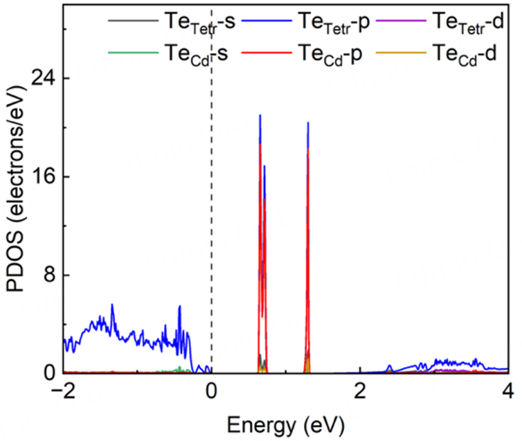
Figure 3. Partial density of states (PDOS) for Te atoms of the defect complex. TeTetr denotes the four tetrahedrally coordinated Te neighbors. These atoms contribute a larger portion of the defect levels, whereas the TeCd antisite defect itself contributes a relatively smaller portion.
The analysis shows that the four neighboring Te atoms make a larger contribution to the defect levels than the central antisite atom itself. Among the contributions of the four tetrahedrally coordinated Te atoms, a small portion comes from the s-orbital, while the overwhelming majority is derived from the p-orbital. For the central Te atom, the contribution comes primarily from the p-orbital, followed by the d-orbital, with a small contribution from the s-orbital. PDOS analysis reveals that the electronic states of the central Te antisite atom and its four coordinated Te atoms overlap, giving rise to the defect-state energy levels E1, E2, and E3. It is evident that the p orbitals of the ligands contribute to bonding with a minor portion of d orbitals. Additionally, the p orbitals of the central Te atom participate in bonding with a small fraction of s orbitals. The PDOS analysis further confirms the strong electron state localization of this defect complex.
To elucidate the spatial distribution of the defect states, the partial charge density (PCD) corresponding to the energy range of the defect levels was visualized in Figure 4.
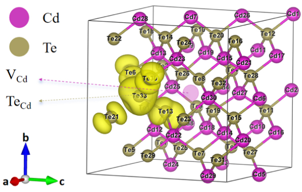
Figure 4. Partial charge density (PCD) of the [VCd-TeCd] complex. Atom Te33 is the TeCd antisite center, and the light pink sphere marks the VCd site. The yellow translucent regions at the 0.005 isosurface around Te33 show charge localization on both the Te antisite atom and its four surrounding Te atoms. This indicates that the defect level originates from the Te antisite atom's electrons combined with the ligand effect induced by the defect.
In Figure 4, the purple and gold spheres represent Cd (numbered 1-30) and Te (numbered 1-33) atoms, respectively. Atom Te33 is identified as the TeCd antisite center, with a VCd vacancy located 4.52 Å away on the (111) plane. The PCD distribution originating from this defect center is visualized at an isosurface level of 0.005, appearing as yellow translucent regions surrounding the Te33 atom. It can be observed that the charge is localized on both the antisite Te atom and its four surrounding Te atoms, indicating that defect energy level arises from a combination of electrons on the antisite atom itself and the ligand effect induced by the antisite defect. The antisite Te atom occupies a Cd site but possesses a different atomic radius and number of valence electrons than Cd. This causes the p-orbitals of the four Te ligands to reorganize, and these recombined orbitals interact with those of the central antisite Te atom, thereby generating defect energy levels within the band gap that are predominantly governed by the ligand orbital characteristics. The collective contribution of these ligand orbitals manifests in the DOS as a larger portion of the defect energy levels, which is consistent with the PDOS results.
To verify the degree of charge localization and distribution morphology around the [VCd-TeCd] complex, the calculated results of the electron localization function (ELF) are shown in Figure 5. Figure 5A presents the ELF distribution of the defect-free crystal. Around the Te atoms, the ELF value reaches approximately 0.8, with a nearly spherical symmetric morphology.
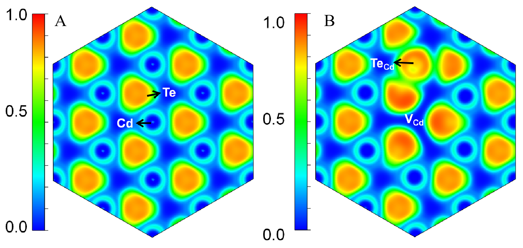
Figure 5. Electron localization function (ELF). (A) The perfect CdTe lattice. (B) The lattice containing [VCd-TeCd] complex.
An ELF value close to 1 indicates strongly localized electrons, with wavefunctions confined to specific atomic sites. ELF ≈ 0.5 corresponds to nearly free-electron-like behavior, where electrons move within the periodic potential of the crystal lattice. In contrast, ELF ≈ 0 represents fully delocalized electrons, whose wavefunctions extend throughout the entire crystal.
Figure 5B shows the ELF plot of the crystal containing the defect complex. Compared with the defect-free crystal, the ELF value around the central Te antisite atom is relatively high (> 0.8), with the ELF distribution displaying an asymmetrical electron distribution localized on each ligand Te atom, pointing toward the Te antisite center. This morphology exhibits electron localization concentrated toward the defect. ELF value between Te antisite center and its nearest-neighbor Te atoms is also higher (ELF = 0.5) than the corresponding region of the defect-free crystal, indicating that the coupling between the central atom and its ligands is taking place through electrostatic interaction. At the VCd vacancy site, the ELF value drops to nearly zero. In contrast, the surrounding Te atoms exhibit high-ELF regions (> 0.8), characterized by a slightly oriented variation toward the vacancy. ELF morphology containing [VCd-TeCd] complex reveals the central Te atom hosts highly localized electrons, while the four ligand Te atoms exhibit a directional electron distribution pointing toward the Te antisite center. The asymmetric defect composed of the VCd vacancy and the Te antisite generates a local electric dipole. This dipole moment not only acts as an additional scattering center, impairing carrier transport efficiency, but also binds charge carriers, leading to a reduced carrier lifetime.
To quantify the specific value of atomic-scale charge transfer, Bader charge analysis was performed, and the results are shown in Figure 6. The vertical axis denotes the electron gain/loss number: positive values correspond to electron gain, and negative values to electron loss. The atom labels on the horizontal axis are identical to those used in the PCD plot [Figure 4]. In Figure 6A the position of purple spheres represents the number of electrons lost by each Cd atom in the defect-free crystal, while that of the blue squares represents those lost by Cd atoms in the defective crystal. Further insight into charge redistribution can be gained by examining the behavior of atoms far from the defect. Cd atoms located far from the [VCd-TeCd] complex exhibit increased electron loss compared to their counterparts in the perfect crystal. This indicates that these distant sites have lost additional electrons. Within the constraints of a charge-neutral supercell, these electrons must be redistributed elsewhere. Given that the [VCd-TeCd] complex carries positive charges, it naturally acts as an electrostatic attractor for these displaced electrons. Consistent with this picture, the near-defect region shows evidence of electron accumulation: Cd atoms adjacent to the defect exhibit reduced electron loss. ELF analysis reveals highly localized electron distributions near the [VCd-TeCd] complex. Thus, a consistent picture emerges of electron transfer from the distant region to the vicinity of the positively charged defect complex, where they become localized and contribute to the formation of the defect states.
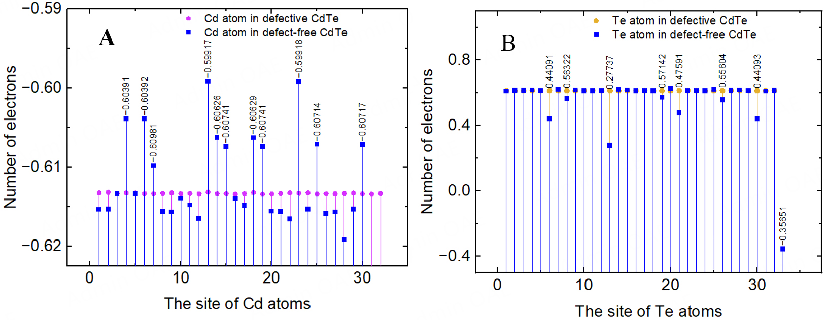
Figure 6. Bader charge analysis of the CdTe supercell. (A) Electron loss by Cd atoms in the defect-free (purple circles) and defective (blue squares) crystals; Cd atoms located far from the [VCd-TeCd] complex lose more electrons than their counterparts in the defect-free crystal, indicating electron accumulation in the Cd atoms adjacent to the defect. (B) Electron gain by Te atoms in the defect-free (gold circles) and defective (blue squares) crystals. All Te atoms in the vicinity of the defect exhibit reduced electron gain.
Figure 6B presents the Bader charge analysis for Te atoms. While regular Te sites remain unaffected, the TeCd antisite center (Te33) loses 0.35651|e| due to its occupation of a cation site. All Te atoms in the vicinity of the defect exhibit reduced electron gain. The quantitative results are as follows, near the Cd vacancy: Te8
In summary, the simulation results show that electrons are accumulated at and around the defect complex and are highly localized, leading to the complex defect donor-like. The orbitals of Te antisite atom and the four Te ligands contribute to three defect levels. Among them, E1 (0.6522 eV above the VBM) and E2
Analysis of element chemical states by XPS
To investigate the chemical states of Cd and Te, XPS was used to analyze different positions of the CdTe ingot, with the results shown in Figure 7. The survey spectra in Figure 7A indicate a high-purity composition, only carbon and oxygen (from the crucible and air, respectively) are observed as impurities. Compared with the other two regions, the middle part of the crystal exhibits lower XPS signal intensities but higher C 1s and O 1s peak intensities, indicating the presence of surface contamination. Therefore, the crystal from the top part of the ingot was used in the subsequent experiments, as it has been shown to exhibit superior quality compared to the tail part based on our previous studies.
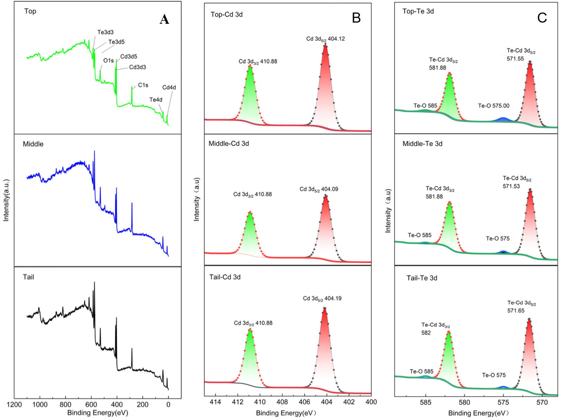
Figure 7. XPS spectra of the CdTe single crystal at different ingot positions. (A) Survey spectra. (B) Cd 3d spin-orbit doublets. (C) Te 3d spin-orbit doublets. A small amount of Te4+ chemical state is observed on the surface of crystals. The binding energies of Cd 3d and Te 3d confirm that they correspond to the chemical states of Cd and Te in CdTe. The Cd: Te atomic ratios at the top, middle, and tail of the ingot are 0.9875:1, 1.0552:1, and 1.0048:1, respectively.
Figure 7B exhibits the Cd 3d binding energy spectra at top, middle, and tail ingot. The Cd 3d orbitals exhibit clear spin-orbit splitting doublets, with the Cd 3d5/2/ characteristic peaks located at 404.12, 404.09, and
Figure 7C shows the Te 3d binding energy spectra. The Te 3d orbitals also exhibit well-resolved spin-orbit splitting doublets, with the Te 3d5/2 characteristic peaks located at 571.55, 571.53, and 571.65 eV, respectively. The spin-orbit splitting energy of Te 3d at top, middle, and tail ingot is 10.33, 10.35, and 10.35 eV, respectively, which are consistent with the spin-orbit splitting energy of the Te 3d level (10.39 eV) and Te 3d5/2 peak at 572.3 eV[26]. However, the chemical state of Te is highly sensitive to environmental and treatment conditions. Ramiro et al. reported that the binding energy of Te 3d5/2 is 573 eV in as-grown CdTe, 572.75 eV in ion-sputtered CdTe, and 575.9 ± 0.2 eV in TeO2[27]. Werthen et al. showed that the Te 3d5/2binding energy was 573.4 eV in a CdTe sample cleaved in dry nitrogen. After 2 h of air exposure, the
Based on the integrated intensities of the Cd 3d and Te 3d doublets, the relative atomic concentrations of Cd and Te in CdTe can be calculated according to the formula
Positron annihilation lifetime (PAL) analysis
Based on the theoretical demonstration that the supercell energy is minimized when the crystal contains only the [TeCd-VCd] complex, a two-state model was thereby adopted in the positron annihilation analysis. In this framework, only one type of dominant defect [TeCd-VCd] complex, in addition to the defect-free lattice, is considered. Positrons exist in two states within the crystal: the free state and trapped state. The free state refers to the state where they move freely in the interstitial positions of the perfect lattice, characterized by an annihilation rate λf = 1/τf0, where τf is the free-state annihilation lifetime, in many literature, it is regarded as the bulk lifetime τb[30]. Trapped state refers to the state that positrons are bound at defects, characterized by an annihilation rate λd = 1/τd, where τd is the trapping-state annihilation lifetime. Since the electron density at defects differs from that in the defect-free lattice, the lifetime τd of the trapped state is different from the lifetime τf of the free state.
The positron annihilation spectrum of CdTe consists of three components: a short-lived component τ1 of 100 ps with an intensity of 12.75, an intermediate component τ2 of 251.10 ps with an intensity of 87.03%, and a long-lived component τ3 of 1,780.00 ps with an intensity of 0.22%. Here, τ1 is taken as the defect lifetime τd, serving as a direct probe of the defect's characteristics, such as their concentrations and the local structural state. This lifetime is far shorter than that related to the A centers in In- or Cl-doped CdTe (320-330 ps)[31,32]. These A centers consist of a group-II vacancy paired off with either a group-VII donor (F, Cl, Br, I) on the Te site, or with a group-III donor (e.g., Ga, In) on the Cd site[33]. The short lifetime observed in the experiment is primarily attributed to the fact that our defect type differs from that of the A centers. The specific reasons will be discussed subsequently. The τ₂ is taken as the bulk lifetime of CdTe, which approximates the free-state lifetime τf. Experimental studies have reported that the positron annihilation bulk lifetime in CdTe lies in the range of 280-290 ps[31,34,35]. One noteworthy study reported that for Cl-doped CdTe, the annihilation lifetime increased from 281 ps in the unannealed state to 294.5 ps after Te-atmosphere annealing[36]. This increase was attributed to the high concentration of Cd vacancies introduced by Te-atmosphere annealing, which rendered the crystal p-type conductive. The CdTe in this study exhibits n-type conductivity with a high average electron concentration, resulting in a shorter bulk lifetime than those reported in the references above. At the same time, the high intensity of this component (I2 = 87.03%) indicates that most positrons annihilate in the bulk state, suggesting that the sample possesses a high-quality lattice structure. τ3 with a very weak intensity was resolved, which is attributed to positron trapping at a low concentration of large open volumes. Given its negligible intensity, this component does not significantly affect the overall trapping kinetics. Therefore, the two-state trapping model was applied using the dominant defect-related component τ1 to estimate the defect complex concentration.
In the two-state trapping model, the annihilation rate of positrons in the free state, λf, is given by λf = πr02cne, where r0 is the classical electron radius, c is the speed of light, and ne is the local electron density at the annihilation site. This equation describes positron annihilation in the free state. It demonstrates that the annihilation rate is independent of the positron velocity and depends solely on, and is directly proportional to, the local electron density at the annihilation site: a higher electron density leads to a higher annihilation rate. Given that the annihilation rate is inversely proportional to the positron lifetime (λ = 1/τ), a shorter lifetime at a specific site implies a higher local electron density.
In theoretical calculation section, Bader charge analysis reveals an accumulation of electrons surrounding the [TeCd-VCd] complex. In addition, ELF analysis indicates that these accumulated electrons are localized at the complex. The synergistic findings of these two analyses indicate an increase in the local electron density at the [TeCd-VCd] complex. Furthermore, the finding reveals that E1 and E2 are donor-type energy levels, which act as hole traps. Because the positron is positively charged, it tends to be trapped by these defect states. Therefore, the increase in local electron density enhances the positron annihilation rate, consequently shortening the positron lifetime to 100 ps. Combined with the simulation analysis, it is reasonable to believe that if the density of [TeCd-VCd] complex is relatively high, the probability of positron annihilation with electrons will be correspondingly increased.
The relationship between the positron trapping rate and defect concentration is given by λd = χd·Cd, where λd (in ns-1) is the trapping rate, Cd is the defect concentration, and χd is the specific trapping coefficient of the defect for positrons. λd was calculated using the two-state trapping model:
XAFS analysis
XANES is defined as the spectral region extending from approximately 30 eV below to 50 eV above an absorption edge[38]. In this energy range, the excited photoelectron possesses a low kinetic energy and consequently a long mean free path, where multiple scattering dominates. This portion of the signal is highly sensitive to the chemical state, coordination environment, and local geometry distortion for the X-ray absorbing atom. Figure 8A shows the Te K-edge XANES spectrum of the CdTe sample. It shows the variation in the Te K-edge absorption coefficient of the sample relative to those of Te foil and TeO2. The X-ray absorption edge energies of the Te element in the CdTe, Te foil, and TeO₂ are 31,813.52, 31,814.42 and 31,817.00 eV, respectively. This absorption edge shows no significant deviation from 31,814 eV of CdTe powders with 99.999% purity[39]. The Te K-edge absorption energy of CdTe is 0.90 eV lower than that of Te foil. This negative shift is characteristic of Te in the Te2- state within II-VI compound semiconductors[40]. This is because the increased numbers of outer-shell electrons enhance shielding, reducing the binding energy of inner-shell electrons and thus lowering the absorption edge energy. These results confirm that Te in CdTe exists as Te2-, where it forms bonds with Cd.
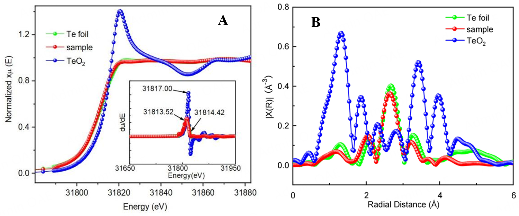
Figure 8. The comparison of Te K-edge X-ray absorption fine structure (XAFS) spectra. (A) X-ray absorption near edge structure spectra. The inset shows the first derivative plot of the absorption coefficient. The absorption edges of CdTe (Te), Te foil, and TeO2 are 31,813.52, 31,814.42 and 31,817.00 eV, respectively. (B) k2 weighted R-space extended X-ray absorption fine structure spectra, shown to compensate for signal attenuation at high wave vector (k) value.
EXAFS refers to the spectral region extending from approximately 30 eV to over 1,000 eV above the absorption edge[41], where the excited photoelectrons have high kinetic energy and predominantly undergo single scattering, providing information on the local atomic structure (e.g., bond lengths and coordination numbers). Figure 8B compares the Te K-edge EXAFS spectra of the CdTe sample, Te foil, and TeO2 in R-space. The horizontal axis R (Å) represents the bond length of different coordination shells, note that the R-space derived from direct Fourier transform of the EXAFS data reflects true interatomic distances. The vertical axis is the Fourier transform magnitude |X(R)|, which reflects both the coordination number and the disorder (σ2) of different coordination shells. The peak centered at about 2.8 Å is due to the first-shell single-scattering (SS) contribution. The structure between about 3.5-6.0 Å is due to the superposition of SS contributions from the second and third shells as well as to non-negligible non-collinear multiple-scattering contributions[39].
The EXAFS spectrum of the sample can be used to analyze the coordination number and bond length.
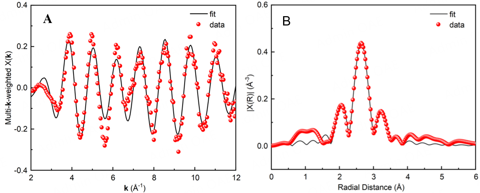
Figure 9. The EXAFS of Te K-edge of sample. (A) EXAFS (points) and fit (line), shown in multi-k-weighted (k1, k2, and k3) k-space. (B) EXAFS (points) and fit (line), shown in multi-k-weighted (k1, k2, and k3) R-space.
To obtain quantitative information of the local structure around the X-ray absorbing atoms, EXAFS analysis was performed in the R-range of 1.8-4.0 Å using three paths, all of which belong to the single-scattering type. The first path corresponds to the first coordination shell based on the cubic zinc-blende crystal structure. In view of the discrepancy between the defects in the actual sample and those documented in the crystallographic database[42], first-principles calculations were carried out on the CdTe crystal structure incorporating TeCd antisite defects, corresponding to the point defect model described in simulation section. The calculated results show that the Muffin-Tin radius (Rmt) between the Te atom and its neighboring Cd atoms in the first shell is 1.361 Å, while that between the antisite Te atom and its neighboring Te atoms in the first shell is 1.474 Å. The second and third paths correspond to the first coordination shell and the second coordination shell scattering paths of elemental Te, respectively. In the curve fits, the coordination numbers and the amplitude reduction factor (S02) were fixed, while all other parameters were set as free parameters. The best-fit structural parameters obtained are presented in Table 1. The corresponding interatomic distance of the first-shell Te-Cd is determined to be 2.79 Å. This value is close to the previously reported DFT simulation value of 2.81 Å[43], around 2.8 Å from 99.9999% purity Te powder[39,44], 2.77-2.82 Å from Fe/Ni-doped CdTe single crystals[40], and 2.65-2.665 Å from Te-Fe doped CdTe[45]. The fitted bond lengths are
Structural parameters for Te K-edge EXAFS for the CdTe
| Paths | Shell | CN | R (Å) | σ2 (Å2) | S02 | R |
| Te-Cd1 in CdTe | Te-Cd1 | 4 (set) | 2.79(5) | 0.021(9) | 0.67 (set) | 0.004 |
| Te-Te1 in elemental Te | Te-Te1 | 2 (set) | 2.81(1) | 0.005(1) | 0.668 (set) | |
| Te-Te2 in elemental Te | Te-Te2 | 4 (set) | 3.47(6) | 0.021(4) | 0.668 (set) |
Single-scattering and three-path fitting were performed using the refined cubic zinc-blende structure model and the trigonal elemental Te model from the Inorganic Crystal Structure Database (ICSD). CN, coordination number. R, interatomic distance. σ2, the Mean Square Relative Displacement. S02, amplitude reduction factor. R, a factor that indicates the goodness of the fit. Data ranges: 3.0 ≤ k ≤ 11.0 Å-1, 1.8 ≤ R ≤ 4 Å.
In XAFS spectroscopy, the core function of wavelet transform is to simultaneously resolve absorption signals in both k-space (energy domain) and R-space (real space). This overcomes the resolution limitations of conventional Fourier transform and enables a more precise characterization of the local atomic coordination environment. Therefore, to further investigate the local structure of Te element, wavelet transform was performed on both the sample and the Te foil, with the results shown in Figure 10.
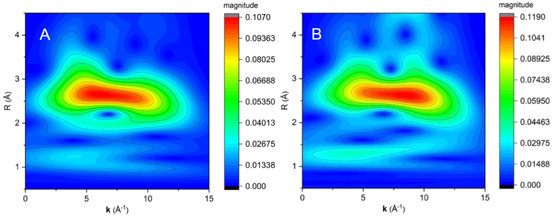
Figure 10. The wavelet transforms. (A) The sample. (B) The Te foil.
The wavelet-transform plots reveal that, in the low k (2-4 Å-1) region corresponding to the low-R side of the first-shell signal, the scattering intensity of CdTe is relatively low, whereas that of Te foil is high. The first coordination shell of CdTe consists of Te-Cd pairs, whereas that of Te foil is composed of Te-Te pairs. Since the scattering amplitude of Cd is weaker than that of Te, the overall scattering intensity of CdTe is lower than that of Te foil. In the medium k (4-8 Å-1) region, corresponding to the main peak position of the first shell, CdTe exhibits a higher scattering intensity compared to Te-Te pairs, indicating that their first-shell geometric structures (bond distance, coordination number, and disorder) are not similar. In the high k
XAFS analysis of the Te K-edge indicates that the chemical state, bond lengths, and coordination numbers in the CdTe single crystal are consistent with the cubic zinc-blende structure. Fitting the experimental data using the calculated crystal model containing TeCd point defects yielded Te-Cd bond lengths in the first coordination shell that are in good agreement with both literature values and theoretical calculations. This suggests that a small number of Te atoms occupy Cd sites, providing strong evidence for the presence of Te antisite defects. The Te-Te bond lengths of the first and second coordination shells are consistent with those of elemental Te, indicating that the crystal contains scattering paths from elemental Te.
CONCLUSION
This paper presents a combination of theoretical calculations and experimental methods to conduct an in-depth analysis of defects in photon-counting-grade CdTe crystals. First, IR transmission microscopy analysis revealed that the Te inclusions in the crystal have sizes mainly in the range of 0-10 μm, with a density of 2.108 × 104 cm-3. Secondly, a [TeCd-VCd] complex point defect model was established using DFT with a U method. Calculations reveal that the dominant defect complex and its surroundings exhibit a higher local electron density than the bulk. These defect-associated electron states introduce donor-type defect energy levels within the bandgap, thereby providing favorable conditions for the trapping of hole-type carriers. XPS analysis indicates that the CdTe (top section) surface is close to stoichiometric composition, with no appreciable contamination. Therefore, the short PAL of 100 ps, attributed to the defect state lifetime, is a result of the presence of locally high-concentration electron densities within the crystal. EXAFS analysis was performed using two structural models: (1) a refined cubic zinc-blende model containing Te antisite defects, which gave a best-fit Te-Cd1 first-shell bond length of 2.79 Å; and (2) an elemental Te model, which gave best-fit bond lengths of 2.81 Å (Te-Te1) and 3.47 Å (Te-Te2) for the first and second coordination shells of Te inclusions.
DECLARATIONS
Acknowledgments
The authors are grateful to Northwestern Polytechnical University for providing the experimental facilities.
Authors’ contributions
Manuscript writing, data analysis, and financial support: Luan, L.
Data processing and fitting: Cheng, Y.
Crystal growth and data acquisition: Zhang, S.
Simulation and calculation, including data acquisition and processing: Zhang, Y.
Discussion and interpretation of the results: Wang, H.; Yang, B.; Zheng, X.; Zhou, Z.
General Supervisor: Wang, T.
Availability of data and materials
The data that support the findings of this study are available from the corresponding author upon reasonable request.
AI and AI-assisted tools statement
Not applicable.
Financial support and sponsorship
The present work was supported by the National Key Research and Development Program of China (Grant No. 2023YFE0108500).
Conflicts of interest
All authors declared that there are no conflicts of interest.
Ethical approval and consent to participate
Not applicable.
Consent for publication
Not applicable.
Copyright
© The Author(s) 2026.
REFERENCES
1. Hou, B.; Chen, Q.; Yi, L.; et al. Materials innovation and electrical engineering in X-ray detection. Nat. Rev. Electr. Eng. 2024, 1, 639-55.
2. Lu, L.; Sun, M.; Lu, Q.; Wu, T.; Huang, B. High energy X-ray radiation sensitive scintillating materials for medical imaging, cancer diagnosis and therapy. Nano. Energy. 2021, 79, 105437.
3. Korotcenkov, G. Handbook of II-VI semiconductor-based sensors and radiation detectors: materials and technology. Cham: Springer International Publishing; 2023.
4. Zhan, X.; Zhang, R.; Niu, X.; et al. Comprehensive evaluations of a prototype full field-of-view photon counting CT system through phantom studies. Phys. Med. Biol. 2023, 68, 175007.
5. Danielsson, M.; Persson, M.; Sjölin, M. Photon-counting X-ray detectors for CT. Phys. Med. Biol. 2021, 66, 03TR01.
6. Grill, R.; Pipek, J.; Iniewski, K.; Betušiak, M. Modelling polarization effects in CdZnTe sensor at low bias. In 2023 IEEE Nuclear Science Symposium, Medical Imaging Conference and International Symposium on Room-Temperature Semiconductor Detectors (NSS MIC RTSD); Vancouver, BC, Canada; 4-11 November 2023; p. 5681.
7. Wang, X.; Wei, T.; Deng, Z. Experimental characterization of an X-ray photon counting detector. J. Inst. 2022, 17, C07005.
8. Xiang, X.; Tong, Y.; Gehrke, A.; Dunham, S. T. Point defects in CdTe and CdTeSe alloy: a first principles investigation with DFT + U. Phys. Rev. Mater. 2024, 8, 084602.
9. Li, Y.; Zha, G.; Guo, Y.; et al. Effects of deep-level traps on the transport properties of high-flux X-ray CdZnTe detectors. Mater. Sci. Semicond. Process. 2021, 133, 105974.
10. Luan, L.; Li, G.; Zhang, S.; et al. Research on point defects in CdTe single crystals. J. Alloys. Compd. 2025, 1037, 182316.
11. Guo, R.; Jie, W.; Wang, N.; et al. Influence of deep level defects on carrier lifetime in CdZnTe:In. J. Appl. Phys. 2015, 117, 094502.
12. Solodin, S.; Panchuk, O.; Fochuk, P. Quasi-chemical analysis of point defect structure іn Mn-doped CdTe single crystals. J. Phys. Chem. Solids. 2020, 138, 109290.
13. Dai, W.; Fu, Z.; Wang, X.; et al. Effects of the distribution of secondary-phase and deep-level defects on the performance of CdZnTe Nuclear radiation detectors. IEEE. Trans. Nucl. Sci. 2025, 72, 1612-9.
14. Malyk, O. The transport phenomena in CdTe:Cl and CdTe:Cu - calculation from the first principles. Phys. Chem. Solid. Stat. 2023, 24, 126-33.
15. Krasikov, D. N.; Scherbinin, A. V.; Knizhnik, A. A.; Vasiliev, A. N.; Potapkin, B. V.; Sommerer, T. J. Theoretical analysis of non-radiative multiphonon recombination activity of intrinsic defects in CdTe. J. Appl. Phys. 2016, 119, 085706.
16. Cola, A.; Dominici, L.; Valletta, A. Electric-field mapping of optically perturbed CdTe radiation detectors. Sensors 2023, 23, 4795.
17. Bezak, M.; Hildén, T.; Kalliokoski, M.; et al. Defects and performance of CdTe and CZT detectors. J. Instrum. 2025, 20, C01021.
18. Robles, R. C.; Torres, V. G. M.; Trinh, C. T.; et al. Multimodal characterization of Te inclusions in Cd1-xZnxTe and Cd1-xZnxTe1-ySey for gamma and X-ray detectors. Sci. Rep. 2025, 15, 31996.
19. Ando, Y. THM growth and characterization of 100 mm diameter CdTe single. IEEE. Trans. Nucl. Sci. 2010, 56, 1717-23.
20. Roy, U.; Bolotnikov, A.; Camarda, G.; et al. Growth of CdTexSe1-x from a Te-rich solution for applications in radiation detection. J. Cryst. Growth. 2014, 386, 43-6.
21. Luan, L.; Zheng, D.; Gao, L.; et al. A large size single crystal growth, scientific evaluation, and giant Faraday effect of cadmium manganese telluride. Mater. Sci. Eng. B. 2022, 283, 115783.
22. Schwarz, R.; Benz, K. Thermal field influence on the formation of Te inclusions in CdTe grown by the travelling heater method. J. Cryst. Growth. 1994, 144, 150-6.
23. Bolotnikov, A. E.; Abdul-Jabbar, N. M.; Babalola, O. S.; et al. Effects of Te inclusions on the performance of CdZnTe radiation detectors. IEEE. Trans. Nucl. Sci. 2008, 55, 2757-64.
24. Jardine, M. J. A.; Dardzinski, D.; Yu, M.; et al. First-principles assessment of CdTe as a tunnel barrier at the α-Sn/InSb interface. ACS. Appl. Mater. Interfaces. 2023, 15, 16288-98.
25. Pochareddy, S. A.; Nicholson, A. P.; Thiyagarajan, A.; Shah, A.; Sampath, W. S. Structural and electronic calculations of CdTe using DFT: exchange-correlation functionals and DFT-1/2 corrections. J. Electron. Mater. 2021, 50, 2216-22.
26. Briggs, D. Handbook of X-ray photoelectron spectroscopy C. D. Wanger, W. M. Riggs, L. E. Davis, J. F. Moulder and G. E. Muilenberg Perkin-Elmer Corp., Physical Electronics Division, Eden Prairie, Minnesota, USA, 1979. 190 pp. $195. Surf. Interface. Anal. 1981, 3, V.
27. Ramiro, J.; Galan, L.; Camarero, E. G. X-ray photoelectron spectroscopy of electrodeposited cadmium mercury telluride thin films and their native surface oxides. J. Mater. Res. 2001, 16, 1942-52.
28. Werthen, J. G.; Häring, J.; Bube, R. H. Correlation between cadmium telluride surface oxidation and metal junctions. J. Appl. Phys. 1983, 54, 1159-61.
29. Ricco, A. J.; White, H. S.; Wrighton, M. S. X-ray photoelectron and Auger electron spectroscopic study of the CdTe surface resulting from various surface pretreatments: correlation of photoelectrochemical and capacitance-potential behavior with surface chemical composition. J. Vac. Sci. Technol. A. 1984, 2, 910-5.
30. Dryzek, J. Remarks on a source contribution in positron lifetime measurements. Nucl. Instrum. Methods. Phys. Res. Sect. B. 2022, 521, 1-6.
31. Corbel, C.; Baroux, L.; Kiessling, F.; Gély-Sykes, C.; Triboulet, R. Positron trapping at native vacancies in CdTe crystals: in doping effect. Mater. Sci. Eng. B. 1993, 16, 134-8.
32. Geffroy, B.; Corbel, C.; Stucky, M.; et al. Detection of non stoichiometric vacancy defects in CdTe, HgTe and Hg1-xCdxTe by positron annihilation. Mater. Sci. Forum. 1986, 10-2, 1241-6.
33. Allen, J. Spectroscopy of lattice defects in tetrahedral II-VI compounds. Semicond. Sci. Technol. 1999, 10, 1049.
34. Keeble, D. J.; Major, J. D.; Ravelli, L.; et al. Vacancy defects in CdTe thin films. Phys. Rev. B. 2011, 84, 5324-6.
35. Fares, N.; Bouarissa, N.; Mezrag, F.; Fares, F. On the behavior of positrons in CdTe under compression. Acta. Phys. Pol. A. 2020, 137, 502-4.
36. Polity, A.; Abgarjan, T.; Krause-Rehberg, R. Investigations of vacancy defects in CdTe by means of positron annihilation. Mater. Sci. Forum. 1994, 175-8, 473-6.
38. Sinfelt, J. H.; Meitzner, G. D. X-ray absorption edge studies of the electronic structure of metal catalysts. Acc. Chem. Res. 2002, 26, 1-6.
39. Abd El All, N.; Dalba, G.; Diop, D.; et al. Negative thermal expansion in crystals with the zincblende structure: an EXAFS study of CdTe. J. Phys. Condens. Matter. 2012, 24, 115403.
40. Sung, N. E.; Park, H. Y.; Jang, M. S. EXAFS analysis of the local structure of Cd(1-x)MxTe (M=Cr, Fe, Ni). AIP. Conf. Proc. 2007, 882, 550-2.
41. Van Bokhoven, J. A.; Lamberti, C. X-ray absorption and X-ray emission spectroscopy: theory and applications. Wiley; 2016.
42. Zachariasen, W. Über die kristallstruktur der telluride von beryllium, zink, cadmium und quecksilber: mit präzisionsbestimmungen der gitterkonstanten. Z. Phys. Chem. 1926, 124U, 277-84.
43. Bhattacharya, S. K.; Kshirsagar, A. Ab initio calculations of structural and electronic properties of CdTe clusters. Phys. Rev. B. 2007, 75, 035402.
44. Abd El All, N.; Thiodjio Sendja, B.; Grisenti, R.; et al. Accuracy evaluation in temperature-dependent EXAFS measurements of CdTe. J. Synchrotron. Rad. 2013, 20, 603-13.
45. Bundaleski, N.; Radisavljević, I.; Ivanović, N.; et al. Local, electronic and surface structure of multi-component Fe-doped CdTe(S) systems. Surf. Sci. 2019, 681, 76-86.
Cite This Article
 Open Access
How to Cite
Download Citation
Export Citation File:
Type of Import
Tips on Downloading Citation
Citation Manager File Format
Type of Import
Direct Import: When the Direct Import option is selected (the default state), a dialogue box will give you the option to Save or Open the downloaded citation data. Choosing Open will either launch your citation manager or give you a choice of applications with which to use the metadata. The Save option saves the file locally for later use.
Indirect Import: When the Indirect Import option is selected, the metadata is displayed and may be copied and pasted as needed.
About This Article
Copyright

Data & Comments
Data
0










Comments
Comments must be written in English. Spam, offensive content, impersonation, and private information will not be permitted. If any comment is reported and identified as inappropriate content by OAE staff, the comment will be removed without notice. If you have any queries or need any help, please contact us at [email protected].