

Tailoring microstructure engineering to decouple electron-phonon transport in Se-based thermoelectric alloys
 0
0 Graphical Abstract
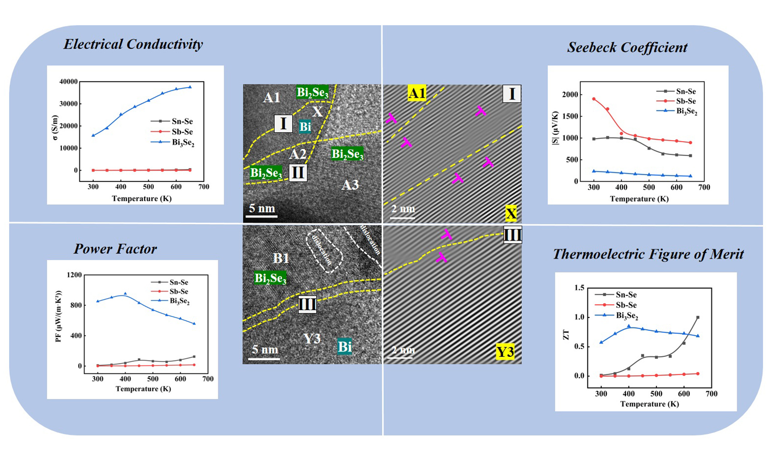
Abstract
Selenide compounds are known for their intrinsically low thermal conductivity, yet their thermoelectric application is often hindered by poor electrical transport. Here we examine how this limitation manifests in three different systems, Sn-Se, Sb-Se, and Bi-Se, by correlating their microstructures with measured transport properties. Sn-Se forms a composite containing crystalline SnSe, elemental Se, and amorphous regions, resulting in ultralow lattice thermal conductivity [0.08 W/(m·K) at 650 K] but limited carrier mobility [~7.39 cm2/(V·s)]. Sb-Se is largely amorphous with scattered Sb2Se3 crystallites, yielding extremely low electrical conductivity (~6.86 × 10⁻² S/m at 300 K) despite a high Seebeck coefficient (1,902 μV/K). Bi-Se develops a distinct two-phase structure comprising metallic Bi nanoprecipitates embedded in a semiconducting Bi2Se3 matrix. This configuration enables efficient charge transport through interconnected Bi pathways [μ ≈
Keywords


 Download PDF
INTRODUCTION
Thermoelectric materials, as functional materials capable of direct conversion between thermal energy and electrical energy, hold significant application value in cutting-edge fields such as industrial waste heat recovery, power sources for space probes, and solid-state refrigeration. Their energy conversion efficiency is governed by the dimensionless thermoelectric figure of merit, ZT = S²σT/κ, where S is the Seebeck coefficient, σ is the electrical conductivity, κ is the total thermal conductivity, and T is the absolute temperature[1]. An ideal thermoelectric material requires both a high power factor (PF = S²σ) and a low thermal conductivity. However, an inherent interdependence exists among these physical parameters[2]: enhancing electrical conductivity by increasing carrier concentration typically leads to a significant reduction in the Seebeck coefficient and a sharp increase in the electronic thermal conductivity. This mutually constraining relationship poses a substantial challenge for the performance optimization of thermoelectric materials.
In recent years, selenium-based thermoelectric materials have been widely investigated due to their unique phonon transport properties and favorable Seebeck coefficients[3]. These materials often exhibit a high intrinsic Seebeck coefficient and low lattice thermal conductivity, demonstrating promising thermoelectric potential[4]. However, the commonly encountered issue of insufficient electrical conductivity severely limits the enhancement of their overall performance[5]. Various selenium-based compounds exhibit significant differences in their microstructures and electro-acoustic transport mechanisms. For example, in SnSe, targeted strategies such as crystal defect engineering (e.g., manipulating intrinsic vacancy defects to enhance phonon scattering[6]) and interface/structure engineering (e.g., tuning crystal symmetry through doping/alloying to decouple electron-phonon transport[7]) have been successfully explored to enhance the power factor while preserving low thermal conductivity. These approaches highlight the potential to optimize thermoelectric transport through precise microstructural manipulation. Hence, clarifying the structure-property relationships in diverse systems will provide critical insights into the fundamental thermoelectric properties and lay the groundwork for devising effective decoupling strategies[8].
Therefore, we select three representative selenide systems, Sn-Se, Sb-Se, and Bi-Se, for a comprehensive investigation of their microstructure and thermoelectric properties by systematic microstructural characterization and thermoelectric performance measurements[9]. While Sn-Se and Sb-Se show limited performance due to insufficient electrical conductivity, the Bi-Se system exhibits exceptional thermoelectric performance originating from a Bi/Bi2Se3 two-phase composite architecture. This unique structure integrates a high-mobility metallic Bi phase for efficient carrier transport and a semiconducting Bi2Se3 matrix for maintaining a reasonable Seebeck coefficient, while interfacial dislocations and disorder strongly scatter phonons[10,11]. Our study highlights an effective semiconductor-metal composite engineering strategy to decouple electrical and thermal transport, providing a viable pathway for designing high-performance selenide-based thermoelectric materials[12].
MATERIALS AND METHODS
Bulk samples of Sn-Se, Sb-Se, and Bi-Se were synthesized via a combined vacuum melting and hot‑pressing approach. High‑purity elemental powders (Sn, Sb, Bi, Se, ≥ 99.99%) were weighed according to the nominal compositions Sn0.51Se0.49, Sb0.41Se0.59, and Bi0.60Se0.40 [Supplementary Figures 1 and 2], and sealed in evacuated quartz tubes (<10-3 Pa). The tubes were heated to 300 °C at 2 °C/min and held for 2 h, then further heated to 650 °C at 1 °C/min and annealed for 12 h, followed by furnace cooling. The obtained ingots were ground into fine powders and consolidated by vacuum hot‑pressing in a graphite die at 450 °C under 5 MPa for 1 h, yielding dense cylindrical pellets (Φ 10 mm × ~10 mm) with relative densities above 95%.
Seebeck coefficient (S) and electrical conductivity (σ) were measured using a Cryoall CTA analyzer (Ar atmosphere, negative pressure). Thermal diffusivity (D) was obtained by laser flash analysis (Netzsch LFA-467). Total thermal conductivity (κ) was derived from κ = D·ρ·Cp, where D, ρ, and Cp denote thermal diffusivity, density, and specific heat capacity, respectively. Carrier concentration (n) was determined by Hall-effect measurements under ambient conditions. The mobility (μ) was calculated by the equation σ = neμ. The crystallinity and composition of the samples were examined by X-ray diffraction (XRD) (λ = 0.154 nm,
RESULTS AND DISCUSSION
X-ray photoelectron spectroscopy (XPS) was employed to investigate the surface chemical states and bonding environments of the three systems. As shown in Figure 1, the Bi 4f spectrum of the Bi-Se system displays characteristic doublet peaks at 158.53 eV (Bi 4f7/2) and 163.85 eV (Bi 4f5/2), corresponding to Bi-Se bonds in the Bi2Se3 phase. A weaker doublet at 157.8 eV and 162.9 eV, positively shifted by about 0.8 eV relative to standard metallic Bi, indicates interfacial charge transfer between metallic Bi nanoparticles and the p-type Bi2Se3 matrix - consistent with the metallic Bi diffraction observed by XRD [Supplementary Figure 3][13]. In the Sb-Se system, the Sb 3d5/2 binding energy at 529.90 eV and the main Se 3d peak at 54.5 eV both confirm Sb-Se bonding, supporting the single-phase Sb2Se3 structure[14]. For the Sn-Se system, the Sn 3d5/2 peak at 486.93 eV is characteristic of Sn-Se bonds in SnSe, while the Se 3d doublet (54.20 eV and 55.18 eV) reveals two distinct chemical environments for Se, corroborating the SnSe/Se composite phase identified in XRD[15]. These XPS results elucidate the distinct bonding nature of each system at the atomic scale: Sb-Se as a single-phase compound, Bi-Se as a metal-compound (Bi2Se3/Bi) composite, and Sn-Se as a compound-elemental selenium (SnSe/Se) composite, providing a foundation for further microstructural analysis by transmission electron microscopy[16,17].
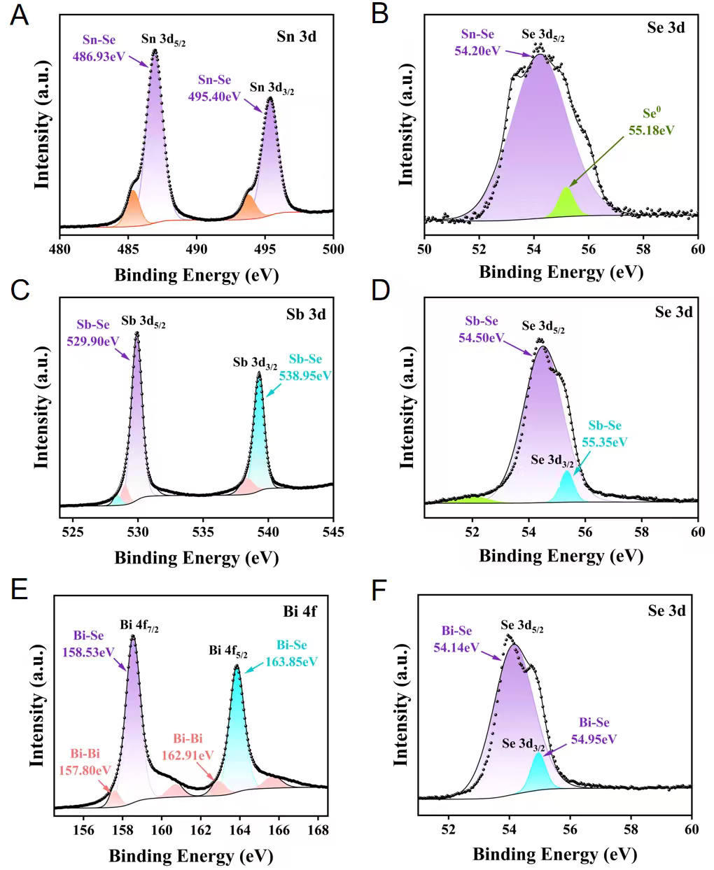
Figure 1. X-ray photoelectron spectroscopy (XPS) spectra of (A) Sn 3d and (B) Se 3d for Sn-Se; (C) Sb 3d and (D) Se 3d for Sb-Se; (E) Bi 4f and (F) Se 3d for Bi-Se.
Figure 2 systematically presents the temperature-dependent thermoelectric properties of the Sn-Se, Sb-Se, and Bi-Se systems. As shown in Figure 2A, the ranking of κL is not constant with temperature. Sn-Se has the lowest κL up to ~450 K, but above ~500 K, Bi-Se becomes the lowest. Sb-Se remains the highest across most of the temperature range. The electronic thermal conductivity κe [Figure 2B] is dominated by Bi-Se due to its high electrical conductivity, contributing significantly to the total κ [Figure 2C]. Bi-Se maintains a moderate total κ [0.45-0.61 W/(m·K)], whereas Sn-Se exhibits an ultralow κ
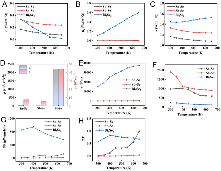
Figure 2. Thermoelectric properties of Sn-Se, Sb-Se and Bi-Se samples. Temperature-dependent profiles of (A) lattice thermal conductivity (κL), (B) electronic thermal conductivity (κe), (C) thermal conductivity (κ), (D) carrier mobility (μ) and carrier concentration (n), (E) electrical conductivity (σ), (F) Seebeck coefficient (S), (G) power factor (PF), and (H) dimensionless figure of merit (ZT).
Conversely, Sb-Se shows extremely low σ (< 0.1 S/m), and Sn-Se exhibits σ ranging from 8.8 S/m at 300 K to 350 S/m at 650 K. The Seebeck coefficient S [Figure 2F] is highest for Sb-Se (1,902 μV/K at 300 K) and Sn-Se (979 μV/K at 300 K), but lower for Bi-Se (233 μV/K at 300 K) due to its high carrier density. Consequently, the power factor PF [Figure 2G] is the highest in Bi-Se, reaching a maximum of ~953 μW/(m·K2) at 400 K. Ultimately, the dimensionless figure of merit ZT [Figure 2H] peaks at ~0.85 around 400 K for Bi-Se, remaining above 0.6 up to 650 K. Sn-Se achieves ZT ~1.0 at 650 K, while Sb-Se shows negligible ZT due to its extremely low σ. The concurrent high σ and moderate κ in Bi-Se signify effective decoupling of electrical and thermal transport, attributable to its unique composite microstructure[18,19].
To elucidate the thermoelectric properties of Sn-Se, transmission electron microscopy (TEM) was employed. Multi-scale images (Figure 3A-C, 50 nm to 5 nm) confirm its composite nature. Lattice analysis of regions in Figure 3C [Figure 3D-G] identifies SnSe in A1 [0.209 nm, (020)], A2 [0.294 nm, (400)], elemental Se in A3 [0.212 nm, (002)] and A4 [0.311 nm, (111)]. Dislocation maps [Figure 3H-K] reveal sparse dislocations in SnSe [Figure 3I] but a high density in Se [Figure 3K], forming a multi-scale phonon-scattering network central to its ultralow lattice thermal conductivity. Further imaging [Figure 3L-M] shows coexisting crystalline and amorphous phases. The crystalline/amorphous interface [Figure 3N] exhibits atomic disorder and dislocation accumulation, further enhancing phonon scattering. Regions B1-B4 in Figure 3M are identified as SnSe via lattice analysis [Figure 3O-R], with spacings of 0.248 nm (401), 0.358 nm (201),
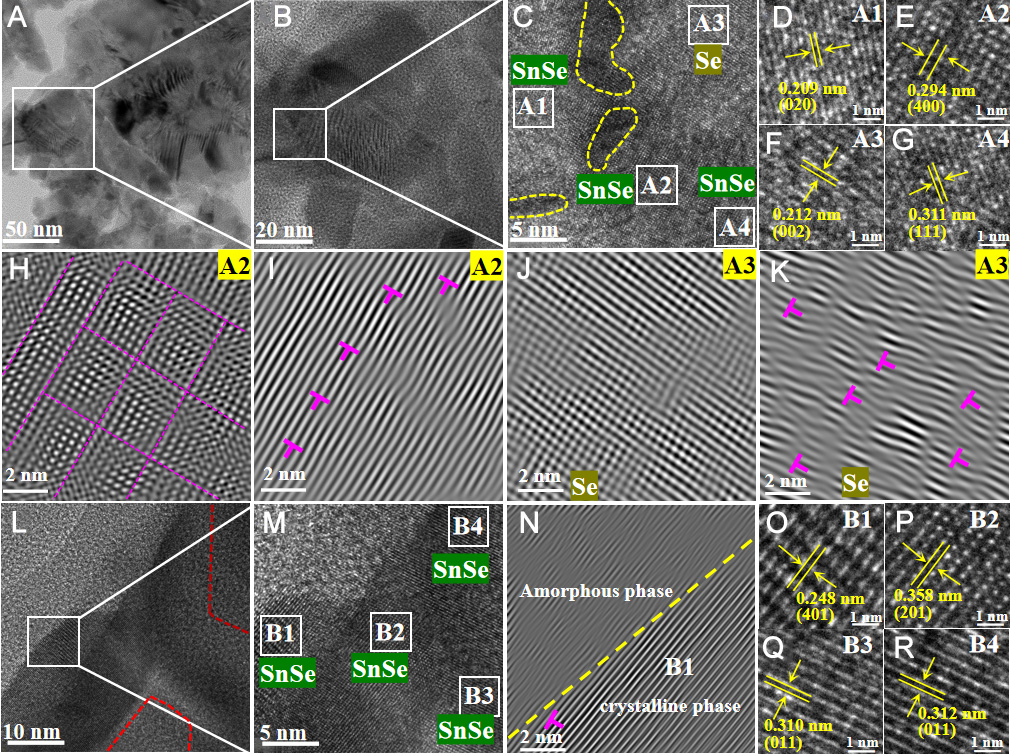
Figure 3. Microstructure characterization of the Sn-Se system. (A-C) TEM images at successively higher magnifications: 50, 20, and 5 nm scales; (D-G) Lattice analysis diagrams corresponding to regions A1, A2, A3, and A4 in (C), respectively; (H and I) Atomic arrangement and dislocation diagrams for region A2; (J and K) the corresponding diagrams for region A3; (L and M) TEM images at 10 nm and 5 nm scales, respectively; (N) Atomic dislocation diagram at the interface between the crystalline region B1 and the amorphous domain; (O-R) Lattice analysis diagrams for regions B1 to B4 in (M). TEM: Transmission electron microscopy.
The presence of the amorphous phase and the high density of defects at the crystalline/amorphous interfaces impose strong scattering on charge carriers. As a result, this leads to a marked reduction in carrier mobility to approximately 7.39 cm2/(V·s) and a correspondingly low electrical conductivity of only 8.76 S/m at 300 K, while simultaneously reducing lattice thermal conductivity[22]. This provides profound insight into the complex trade-off between electrical and thermal transport parameters in the Sn-Se system: the abundant phase interfaces and defect structures effectively suppress phonon transport but inevitably impede the directional migration of carriers, yielding poor electrical conductivity[23]. The Seebeck coefficient of the Sn-Se system exhibits a systematic temperature dependence, decreasing from 979.7 μV/K at 300 K to 594.4 μV/K at 650 K. Although the Seebeck coefficient decreases with increasing temperature, its absolute value remains relatively high at 650 K. This is attributed to the moderate carrier concentration in the system, which avoids the severe degradation of the Seebeck coefficient typical of heavy doping while still providing sufficient carriers for transport[24].
TEM analysis of the single-phase Sb2Se3 system reveals a microstructure dominated by an amorphous matrix with embedded crystalline domains [Figure 4A-C]. Lattice analysis of Figure 4C confirms the crystalline regions as Sb2Se3, region A1 exhibits spacings of 0.601 nm (020) and 0.324 nm (230) [Figure 4D], region A2 shows 0.601 nm (020) [Figure 4E], region A3 shows 0.312 nm (211) [Figure 4F], and region A4 shows
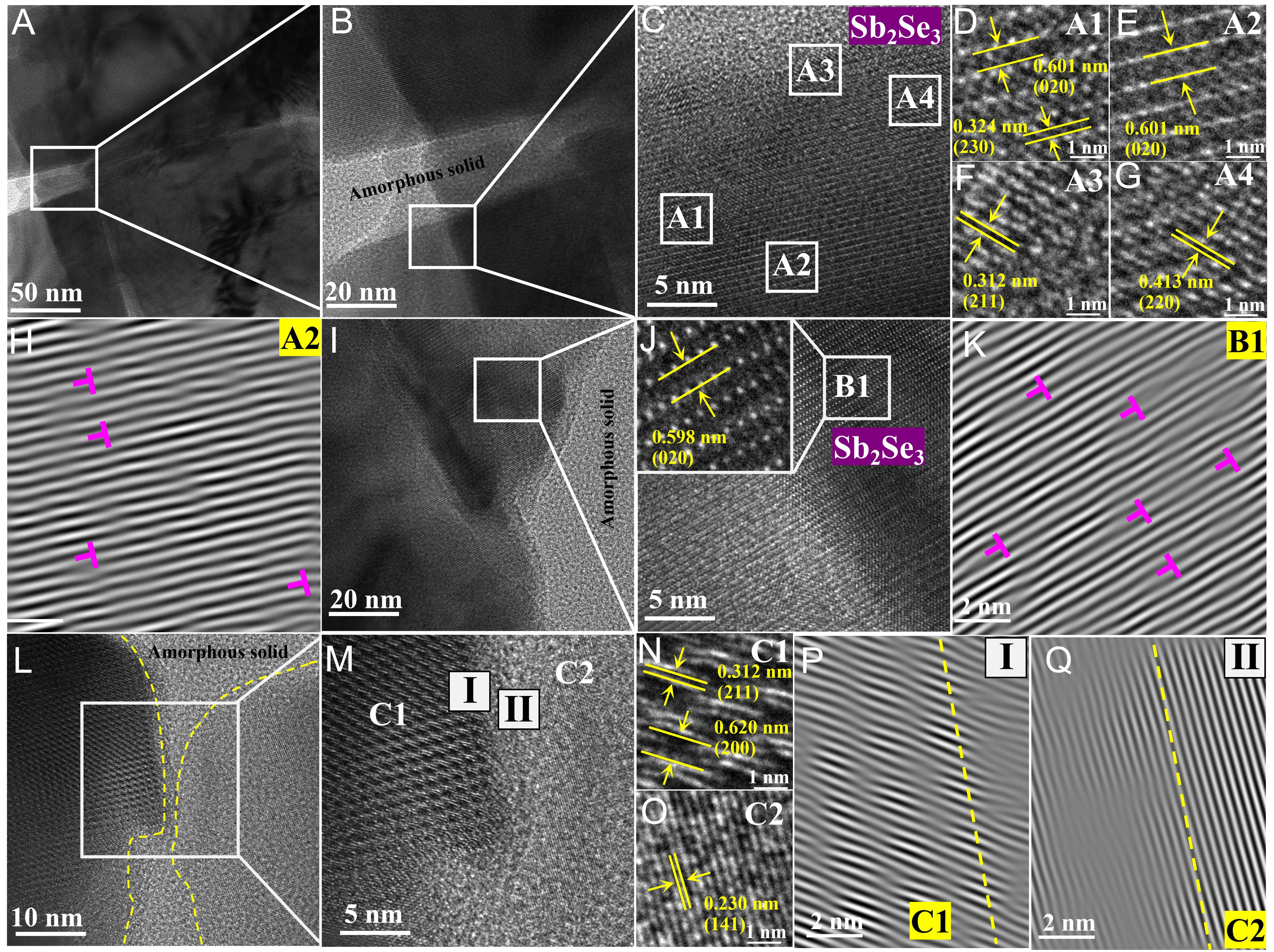
Figure 4. Microstructure characterization of the Sb-Se system. (A-C) TEM images at progressively higher magnifications: 50, 20, and
This specific structure dictates its thermoelectric properties. The high amorphous fraction (evident in Figure 4B, I and L) strongly suppresses phonon transport, yielding a low lattice thermal conductivity of
TEM reveals the nanocomposite structure of the Bi-Se system. Multi-scale images (Figure 5A-C, 50 nm to
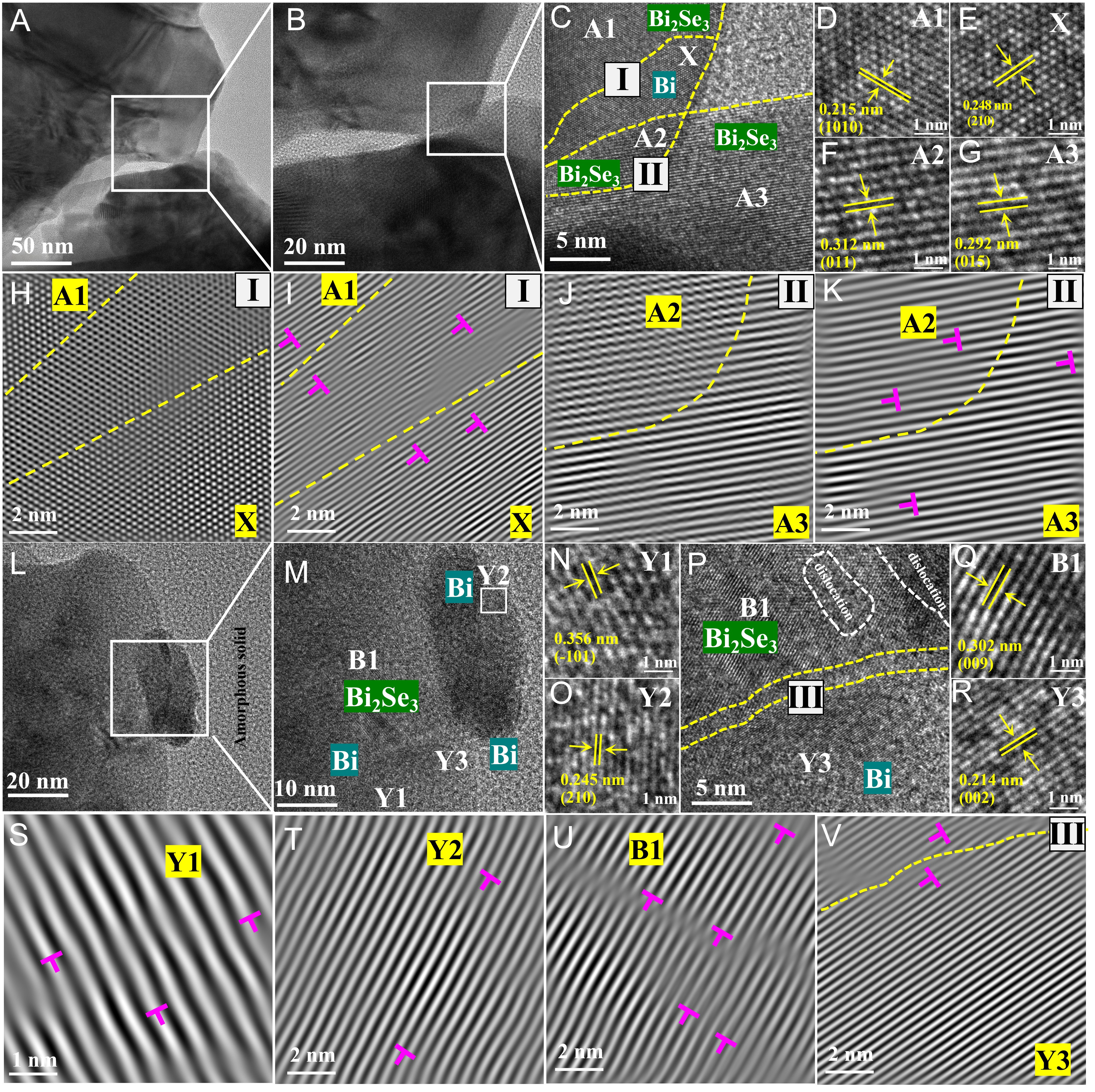
Figure 5. Microstructure characterization of the Bi-Se system. (A-C) TEM images at successively higher magnifications: 50, 20, and 5 nm scales; (D-G) Lattice analysis diagrams corresponding to regions A1, X, A2, and A3 in (C), respectively; (H and I) Atomic arrangement and dislocation maps for region I; (J and K) the corresponding maps for region II; (L and M) Additional TEM images at 20 nm and 10 nm scales; (N and O) Lattice analysis diagrams for regions Y1 and Y2 in (M); (P) Additional TEM image at 5 nm scale; (Q and R) Lattice analysis diagrams for regions B1 and Y3 in (P); (S-V) Atomic dislocation maps for region Y1, region Y2, region B1, and region III, respectively. TEM: Transmission electron microscopy.
Although the relatively high carrier concentration and small effective mass (0.068 m0) impose certain limitations on the Seebeck coefficient, the synergistic optimization of electro-phonon transport, combining the high conductivity of metallic Bi, the sustained Seebeck coefficient from the Bi2Se3 phase, and the strong phonon scattering at the two-phase interfaces, collectively enables Bi-Se to deliver excellent thermoelectric performance over a wide temperature range, with a peak ZT of approximately 0.85 at 400 K)[29,30].
CONCLUSION
We systematically compared the thermoelectric performance and microstructures of Sn-Se, Sb-Se, and Bi-Se. Sn-Se and Sb-Se are limited by low electrical conductivity; however, Sn-Se achieves a ZT of ~1.0 at 650 K, owing to its ultralow lattice thermal conductivity [~0.08 W/(m·K)] from amorphous Se and abundant crystalline/amorphous interfaces. In contrast, Bi-Se exhibits a peak ZT of ~0.85 at 400 K and maintains ZT > 0.6 up to 650 K. This performance originates from its Bi/Bi2Se3 two-phase composite: metallic Bi precipitates provide high-mobility conduction pathways [μ ≈ 2,170 cm2/(V·s)], while the Bi2Se3 matrix retains a Seebeck coefficient of ~233 μV/K at room temperature. This work demonstrates that semiconductor - metal composite engineering effectively decouples electrical and thermal transport, offering a promising strategy for high-performance selenide-based thermoelectrics.
DECLARATIONS
Authors’ contributions
Writing - original draft; conceptualization; data curation; methodology; formal analysis; investigation: Wang, H.
Writing - review & editing; investigation: Xu, H.
Writing - review & editing; supervision; investigation: Chen, Y.
Writing - review & editing; supervision; resources; project administration; funding acquisition: Wang, G.
Data curation: Shi, H.
Availability of data and materials
The data supporting the findings of this study are available within this Article and its Supplementary Materials. Further data are available from the corresponding authors upon request.
AI and AI-assisted tools statement
Not applicable.
Financial support and sponsorship
This work was supported by the Natural Science Foundation of Ningbo City, China (Grant No. 2022J072), the Zhejiang Provincial Natural Science Foundation of China (Grant No. LD26F050003), the Fundamental Research Funds for the Provincial Universities of Zhejiang (Grant No. SJLZ2024004), and the K. C. Wong Magna Fund at Ningbo University.
Conflicts of interest
All authors declared that there are no conflicts of interest.
Ethical approval and consent to participate
Not applicable.
Consent for publication
Not applicable.
Copyright
© The Author(s) 2026.
Supplementary Materials
REFERENCES
1. Spalva, E.; Niherysh, K.; Andzane, J.; Felsharuk, A.; Erts, D. Interface-induced enhancement of thermoelectric properties of Bi2Se3-n-type MWCNT heterostructures revealed by magnetotransport analysis. J. Alloys. Compd. 2025, 1020, 179299.
2. Jiang, F.; Xia, C.; Zhu, Y.; Li, J.; Chen, Y.; Liu, W. Thermoelectric transport properties of p‐type Bi2Se3-Sb2Se3-In2Se3 high entropy compounds. Rare. Met. 2024, 43, 3415-21.
3. Tang, X.; Wu, L.; Xu, Z.; Liu, L.; Song, Z.; Song, W. Thermal conductivity of selenium crystals based on machine learning potentials. Phys. Chem. Chem. Phys. 2025, 27, 20334-43.
4. Bisht, N.; More, P.; Khanna, P. K.; Abolhassani, R.; Mishra, Y. K.; Madsen, M. Progress of hybrid nanocomposite materials for thermoelectric applications. Mater. Adv. 2021, 2, 1927-56.
5. Yang, R.; Li, X.; Guo, W.; et al. New thermoelectric semiconductors Pb5Sb12+xBi6-xSe32 with ultralow thermal conductivity. Chin. J. Struct. Chem. 2024, 43, 100268.
6. Gong, Y.; Dou, W.; Lu, B.; et al. Divacancy and resonance level enables high thermoelectric performance in n-type SnSe polycrystals. Nat. Commun. 2024, 15, 4231.
7. Chen, Z.; Shi, X.; Zhao, L.; Zou, J. High-performance SnSe thermoelectric materials: Progress and future challenge. Prog. Mater. Sci. 2018, 97, 283-346.
8. Neelakandan, S.; Biswas, K. Composite way to superior thermoelectric performance in in filled Co4Sb12. Solid. State. Sci. 2025, 168, 108028.
9. Yan, Q.; Kanatzidis, M. G. High-performance thermoelectrics and challenges for practical devices. Nat. Mater. 2022, 21, 503-13.
10. Wang, S.; Xiao, Y.; Ren, D.; Su, L.; Qiu, Y.; Zhao, L. Enhancing thermoelectric performance of BiSbSe3 through improving carrier mobility via percolating carrier transports. J. Alloys. Compd. 2020, 836, 155473.
11. Yin, Z.; Zhang, H.; Wang, Y.; et al. Superior carrier mobility enabled by the charge channel leads to enhanced thermoelectric performance in BiCuSeO composites. Small 2023, 19, e2304430.
12. Yang, X.; Liu, Y.; Peng, R.; et al. Discovery of half-heusler alloys with intrinsically low lattice thermal conductivity via the equivalent valence electron principle. ACS. Appl. Mater. Interfaces. 2026, 18, 6723-34.
13. Aziz, M.; Ismail, A. X-ray photoelectron spectroscopy (XPS). In Membrane Characterization; Elsevier, 2017; pp. 81-93.
14. Sharma, J.; Aliev, Z. S.; Mahatha, S. K. Sn deposition on Bi2Se3: interfacial chemistry over stanene growth. Phys. Status. Solidi. RRL. 2025, 20, e202500404.
15. Zhang, Y.; Cheng, L.; Li, L.; et al. ZnSe/SnSe heterostructure incorporated with selenium/nitrogen co-doped carbon nanofiber skeleton for sodium-ion batteries. Small 2024, 20, e2306536.
16. Zhao, H.; Zhu, Y.; Ye, H.; et al. Atomic‐scale structure dynamics of nanocrystals revealed by in situ and environmental transmission electron microscopy. Adv. Mater. 2023, 35, 2206911.
17. Uribe, B. E. B.; Tarpani, J. R. Interphase analysis of hierarchical composites via transmission electron microscopy. Compos. Interfaces. 2017, 24, 849-59.
18. Lancin, M.; Marhic, C. TEM study of carbon fibre reinforced aluminium matrix composites: influence of brittle phases and interface on mechanical properties. J. Eur. Ceram. Soc. 2000, 20, 1493-503.
19. Chen, B.; Shen, J.; Ye, X.; et al. Length effect of carbon nanotubes on the strengthening mechanisms in metal matrix composites. Acta. Mater. 2017, 140, 317-25.
20. Cui, J.; Guo, C.; Zou, L.; Li, C.; Du, Z. Experimental investigation and thermodynamic modeling of the Se-Sn-Te system. J. Alloys. Compd. 2015, 642, 153-65.
21. Tang, Z.; Aoyagi, K.; Nukui, Y.; et al. Reaction path for formation of Cu2SnSe3 film by selenization of Cu-Sn precursor. Sol. Energy. Mater. Sol. Cells. 2015, 143, 311-8.
22. Ran, X.; Zhu, J.; Zhang, C.; Yang, L.; Chen, Y. Hole transportation and defect passivation properties at the perovskite/SAHTM interface: the effect of heteroatom groups and alkyl chain lengths in self-assembled phosphonic acid carbazole derivatives. J. Mater. Chem. C. 2025, 13, 1874-82.
23. Ma, J.; Xu, Y.; Nan, Z.; et al. Modulation for Seebeck coefficient and power factor of flexible PEDOT:PSS films by incorporating SnSe nanosheets and solvents treatment. J. Alloys. Compd. 2025, 1022, 179793.
24. Yadav, M.; Singh, V.; Sharma, S. K.; et al. Temperature driven n- to p-type conduction switching in SnSe and its mitigation through Zn doping with added advantage of Improved thermoelectric performance. Emergent. Mater. 2025, 8, 3753-60.
25. Mo, Z.; Yang, M.; Li, H.; et al. Optimizing thermoelectric performance of Ag2Se via Sb2Se3 addition. Vacuum 2025, 241, 114613.
26. Bude, R.; Divay, L.; Bisaro, R.; et al. Synthesis of alloyed Bi2TexSe3-x nanoparticles and thermoelectric characterization of bulk nanostructured materials obtained by their assembly. MRS. Proc. 2015, 1804, 1-6.
27. Jabar, A.; Abounachit, O.; Idrissi, S.; Bahmad, L. Understanding of strain condition effects on physical properties of the Bi2Se3 compound by the DFT method. J. Supercond. Nov. Magn. 2025, 38, 6912.
28. Musah, J.; Or, S. W.; Kong, L.; Wu, C. L. Al-doped Bi2Se3 nanoparticulate semiconductors with controlled resonance states for enhanced thermoelectric efficiency. Mater. Today. Energy. 2024, 42, 101555.
29. Vijay, V.; Harish, S.; Archana, J.; Navaneethan, M. Ultra-high power factor of p-type Bi2Se3 for room-temperature thermoelectric applications. Chem. Commun. 2023, 59, 8119-22.
Cite This Article
 Open Access
How to Cite
Wang, H.; Wang, G.; Xu, H.; Chen, Y.; Shi, H. Tailoring microstructure engineering to decouple electron-phonon transport in Se-based thermoelectric alloys. Microstructures 2026, 6, 20260126. https://dx.doi.org/10.20517/microstructures.2026.66
Download Citation
If you have the appropriate software installed, you can download article citation data to the citation manager of your choice. Simply select your manager software from the list below and click on download.
Export Citation File
Type of Import
Tips on Downloading Citation
Citation Manager File Format
Type of Import
Direct Import: When the Direct Import option is selected (the default state), a dialogue box will give you the option to Save or Open the downloaded citation data. Choosing Open will either launch your citation manager or give you a choice of applications with which to use the metadata. The Save option saves the file locally for later use.
Indirect Import: When the Indirect Import option is selected, the metadata is displayed and may be copied and pasted as needed.
About This Article
Copyright

Data & Comments
Data
0











Comments
Comments must be written in English. Spam, offensive content, impersonation, and private information will not be permitted. If any comment is reported and identified as inappropriate content by OAE staff, the comment will be removed without notice. If you have any queries or need any help, please contact us at [email protected].