

Tuning terahertz wave absorption in diamond/NdFeB composite films via magnetic interfacial engineering
 0
Graphical Abstract
Abstract
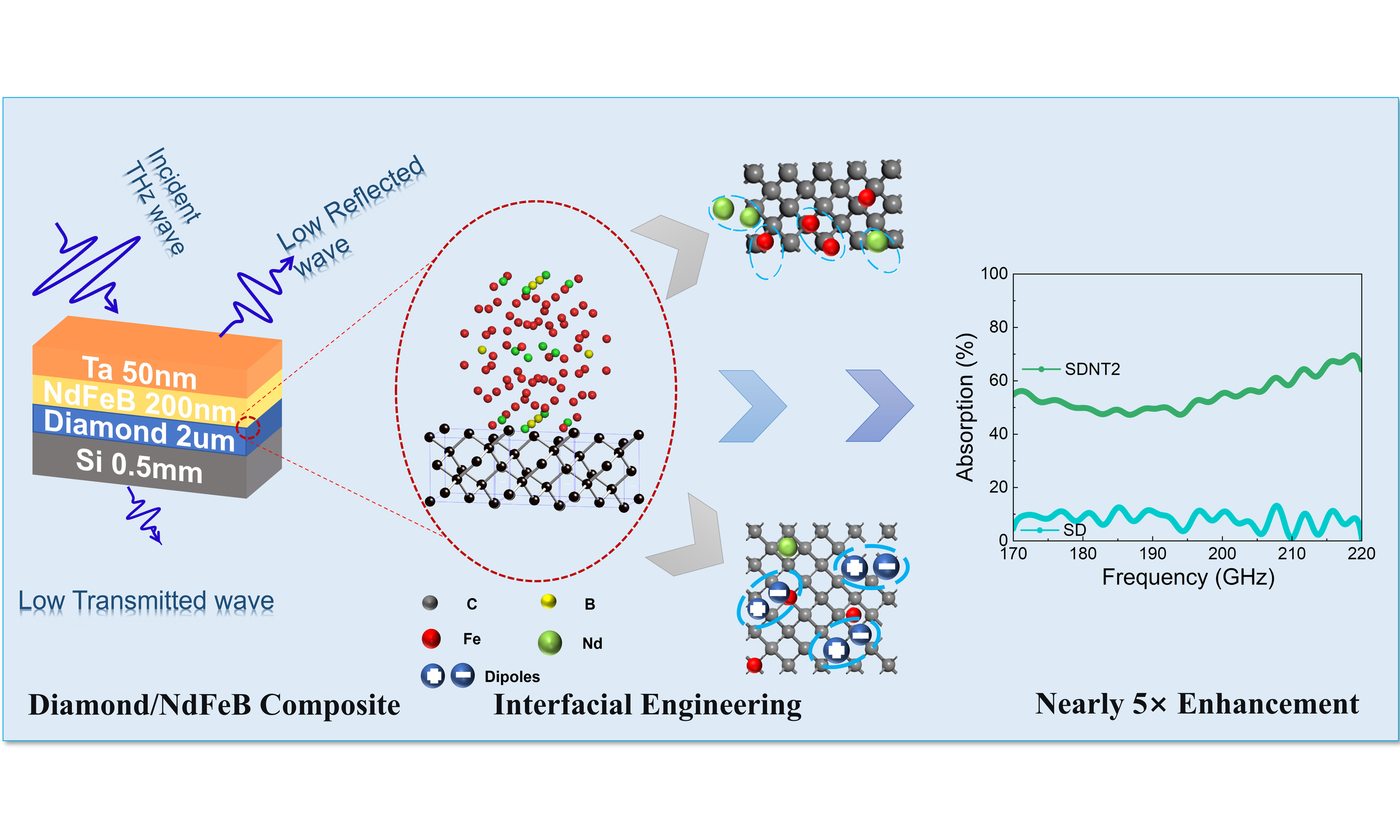
This work endows diamond with effective terahertz absorption capability through interfacial polarization and defect engineering at diamond/NdFeB heterointerfaces, achieved via a combined CVD and magnetron sputtering process. By optimizing the interfacial architecture, specifically, the insertion of a Ta interlayer and the thickness of the magnetic layer, we significantly tuned the dielectric performance and the impedance matching. This modulation stems from the mechanism of interfacial polarization, dipole relaxation and magnetoelectric synergy. When a NdFeB layer of 200 nm thickness was deposited directly onto a diamond substrate, it induced interfacial defects and generated an sp2 carbon network, which served as additional dipolar centers. Interfacial band bending and charge redistribution generate a space-charge region, which in turn establishes an intrinsic interfacial dipole layer, and strengthens interfacial polarization. Consequently, the composite film exhibits a minimum absorptivity exceeding 47% over the 170-220 GHz band with a peak value of 70%, representing a nearly fivefold enhancement over pristine diamond. This work demonstrates a new material paradigm for terahertz absorption by transforming diamond into an effective absorber through interfacial engineering with NdFeB.
Keywords


 Download PDF
INTRODUCTION
The terahertz (THz) band corresponds to the electromagnetic spectrum spanning 0.1 to 10 THz. Situated between microwaves and infrared radiation, it inherits the properties of both frequency regimes while displaying unique merits[1]. Terahertz communication technology covering 170-220 GHz demonstrates great potential for 6G high-capacity and long-distance communications by virtue of an ultra-wide bandwidth and favorable atmospheric penetration, while the distinct attenuation characteristics of different sub-bands enable it to satisfy secure anti-interference communication and point-to-point communication requirements, respectively[2-4]. Featuring broadband and short wavelengths, terahertz electromagnetic waves (TEMW) in this range can significantly improve sensing resolution and are expected to be integrated into 6G smart terminals for extended sensing applications, such as food composition detection and human subcutaneous health monitoring[5-7]. The broad application prospects require THz devices and components to operate reliably in complex environments[8,9]. Therefore, there is a pressing need to explore alternative material design strategies that broaden the available portfolio of terahertz absorbers beyond conventional metallic or carbon-based systems[10,11].
In the field of TEMW absorption, conventional materials generally exhibit significant electromagnetic responses mainly in the gigahertz frequency range[12,13]. Traditional TEMW absorbers often suffer from drawbacks, including poor frequency tunability, narrow bandwidth, and complex structural architecture[14,15]. For single-phase material systems, simultaneously achieving both impedance matching and high loss is extremely challenging: materials with high intrinsic loss (e.g., conductors) usually suffer from severe impedance mismatch, leading to strong surface reflection, while materials with good impedance matching (e.g., dielectrics) often lack sufficient intrinsic loss[16,17]. It is precisely this inherent contradiction that has driven the development of more complex designs, such as composites, metasurfaces, and interface engineering. First, metasurface design has been introduced, which employs artificially engineered sub-wavelength structures to precisely regulate TEMW[18]. However, absorbers of this type provide inherently narrowband absorption. Furthermore, their structural complexity and reliance on precision machining hinder practical applications[19]. Second, novel functional materials, such as graphene, MXenes, VO2 phase-change materials, and Dirac semimetals, have been developed and incorporated into TEMW absorption systems. However, carbon-based nanomaterials suffer from inherent bottlenecks in device integration and fabrication stability[20]. MXenes and Dirac semimetals are prone to oxidation and exhibit poor environmental stability, which easily causes performance failure under variable ambient conditions[21-23]. VO2 is inherently weakened by its high phase-transition temperature, limited operational bandwidth, and restricted tunability[24,25]. Third, composite and interface engineering has been proposed, employing strategies such as the introduction of multiple loss mechanisms, designing gradient dielectric structures, and leveraging interfacial synergy to optimize the impedance matching and the energy dissipation[26-28]. However, this approach also faces problems such as uneven interfacial coupling exacerbating an impedance mismatch, multiple polarizations causing a high-frequency reflection, and thick composite layers leading to structural defects, making it difficult to balance loss and matching effectively.
Unlike diamond-based THz absorbers that rely on complex metasurface designs, and interface-engineering studies confined to the gigahertz band with multilayer stacking[29], this work introduces a diamond/NdFeB composite film fabricated by a straightforward combination of chemical vapor deposition and magnetron sputtering. The directly contacted diamond/NdFeB interface simultaneously activates three synergistic loss mechanisms, including interfacial polarization, defect-dipole relaxation, and magnetoelectric synergy. This self-generated interfacial architecture fundamentally differs from conventional layer-by-layer assembly and offers a new paradigm for terahertz absorption. The low dielectric loss of diamond ensures minimal energy dissipation, which is essential for maintaining device performance[30]. Meanwhile, it also provides structural support under a variety of environments[31]. The NdFeB coating, as the magnetic layer, enables the tuning of electromagnetic parameters and impedance matching through interfacial coupling and thickness variation, thereby enhancing absorption[32,33]. Specifically, the direct interfacial coupling without a barrier layer strengthens the interfacial polarization, introducing multiple dielectric loss mechanisms. The distinct electronegativity difference between diamond and Nd/Fe in NdFeB drives an interfacial electron transfer from the metallic phase to the diamond side, while the bandgap difference between the two materials dictates an interfacial band alignment. The observed structural modifications at the diamond/NdFeB interface are consistent with the charge redistribution expected from the band alignment at this heterojunction. This gives rise to an interfacial dipole layer and a space-charge region that promote carrier separation and strengthen interfacial polarization, thereby contributing to the enhanced dielectric loss[34]. Precise control of the NdFeB layer thickness optimizes the dielectric properties and avoids the impedance degradation typically seen in thick films, while the interfacial coupling effectively mitigates excessive reflection and balances carrier transport with energy dissipation, ultimately achieving a synergistic optimization between impedance matching and electromagnetic absorption.
In this study, films with varied interface structures and NdFeB thicknesses were designed as absorbers for the 170-220 GHz band. The composite film achieved over 47% absorption (up to 70%) in the 170-220 GHz range, markedly surpassing pure diamond. Structural characterization revealed significant lattice distortion, and sp2-carbon defects. Lattice mismatch, and the notable electronegativity difference, introduce strains and charge transfer, building an intrinsic interfacial dipole layer and strengthening the interfacial polarization. The defects act as additional polarization centers, which undergo directional reorientation under terahertz electromagnetic fields inducing defect dipole relaxation. Variations in carrier mobility further confirm the interfacial synergistic effect, manifesting as a reduction in the AC electrical conductivity of the composite thin film and an enhancement in carrier mobility, which significantly improves its TEMW absorption performance. This work aims to transform diamond from a passive transparent medium into an absorbing component by interfacial engineering with NdFeB, and concurrently to improve impedance matching through magnetic modulation, thereby enabling substantial terahertz absorption in a material conventionally considered transparent.
MATERIALS AND METHODS
Synthesis of the composite film
The diamond/NdFeB composite films were fabricated by first depositing a diamond film onto a Si (001) single-crystal substrate (Hefei Kejing Materials Technology Co., Ltd.) via CVD, followed by the growth of an NdFeB film on the diamond layer using magnetron sputtering. Before deposition, the cleaned Si substrates were sonicated for 30 min in a diamond suspension (NanoCarbon Research Institute, Ltd., NanoAmando Colloid) to enhance nucleation. Deposition was conducted at a chamber pressure of 2,000 Pa and a substrate temperature of 770 °C for 3 h, with hydrogen and methane flow rates of 400 sccm and 2 sccm, respectively. For the magnetron sputtering process, a target with a nominal composition of Nd2Fe14B (atomic ratio) was prepared via the powder metallurgy method while Ta target with purity above 99.9% was a commercial product. The deposition rates of Nd2Fe14B and Ta layers were 9.11 and 2.95 Å/s respectively. They were calibrated by monitoring the weight using a Sartorius MP-SC 2 high-precision balance. The base pressure was better than 3 × 10⁻⁵ Pa, while the Ar pressure was kept at 0.1 Pa during sputtering deposition. Deposition was performed at a substrate temperature of 550 °C, after which the samples were subjected to in situ annealing to optimize the structural quality and interfacial properties. Metallic Ta acts as a barrier layer between the diamond and NdFeB films, as well as an oxidation-resistant layer on the surface of all NdFeB samples. The samples were labeled as follows: pure diamond film as Si/diamond (SD), samples without a Ta interlayer as Si/diamond/NFB/Ta (SDNT)2 and SDNT4, and samples with a Ta interlayer as Si/diamond/Ta/NFB/Ta(SDTNT)2. The number following the letters indicates the thickness of the NdFeB layer in nanometers: 2 for 200 nm and 4 for 400 nm.
Characterization
The orientation and phase composition of the films were characterized by Bruker D8 Advance grazing-incidence X-ray diffraction (GIXRD) using Cu Kα radiation (Bruker, Germany). The diamond phase was investigated by Raman spectroscopy (Horiba, Labram HR Evolution instrument, France), employing a 532 nm laser with an 1,800 lines mm-1 grating. The microstructure and elemental composition of the films were characterized by a ZEISS SUPRA 55 field-emission scanning electron microscope (SEM, ZEISS, Germany). Surface morphology and roughness were characterized by a Bruker MultiMode 8 atomic force microscope (AFM) operated in tapping mode. The room-temperature magnetic properties were measured with a vibrating sample magnetometer (VSM, Model 3107, East Changing Technologies, China). Hall-effect measurements were performed at 300 K using a physical property measurement system (PPMS, Quantum Design, USA), with the magnetic field applied perpendicular to the ab-plane. The electromagnetic wave absorption properties in the 170-220 GHz range were characterized using a vector network analyzer (VNA, 3674H, CETC Ceyear Technologies Co., Ltd., China) in a T/R free-space configuration, where the S parameters were recorded and the electromagnetic parameters were subsequently extracted using the NRW inversion algorithm.
RESULTS AND DISCUSSION
Phase and structural analysis and discussion
To clarify the phase composition of the samples, GIXRD characterization was performed, and the results are presented in Figure 1A. By comparing the GIXRD patterns with standard PDF cards, characteristic diffraction peaks corresponding to the (111) and (220) crystal planes of diamond were detected in all samples, confirming the successful crystallization of the diamond phase[35]. A magnified view of the diamond peaks is provided in Figure 1B for detailed comparison. It reveals a shift in the diamond diffraction peaks within the composite films, indicating the presence of lattice strain at the interface. This strain originates from the significant mismatch in both the thermal expansion coefficients and the lattice constants between diamond and NdFeB. The induced stress gives rise to the lattice distortion, which disrupts the periodic potential field of the crystal lattice[36]. This disruption enhances the probability of electron scattering and provides a thermodynamic driving force for the formation of interfacial defects[37].
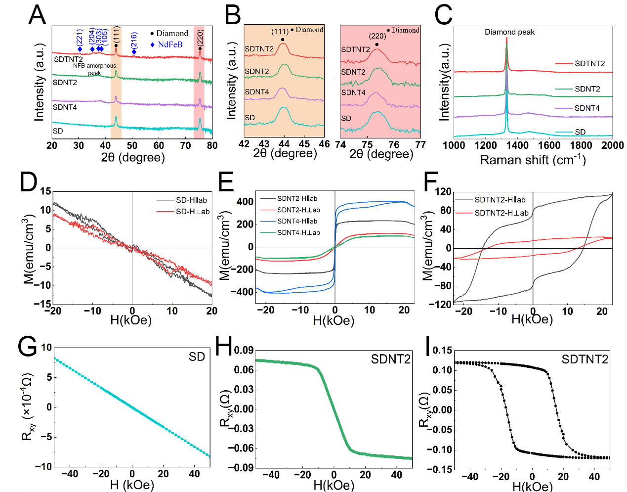
Figure 1. Structure and electromagnetic properties of diamond/NdFeB composite films. (A) GIXRD spectra, (B) magnified XRD spectra of diamond (111) and (220) crystal planes, (C) Raman spectra in the range of 1,000-2,000 cm-1, Room temperature M-H hysteresis loop of (D) SD, (E)SDNT2 and SDNT4, (F) SDTNT2, Room temperature Hall resistance curve of (G) SD, (H)SDNT2, (I)SDTNT2. SDTNT: Si/diamond/Ta/NFB/Ta; SDNT: Si/diamond/NFB/Ta; SD: Si/diamond; GIXRD: grazing-incidence X-ray diffraction.
In addition to the characteristic diffraction peaks of diamond, the SDTNT2 sample displays additional characteristic peaks, such as the (303) and (105) crystal planes of the tetragonal Nd2Fe14B phase [Figure 1A and Supplementary Figure 1]. For the SDNT2 and SDNT4 samples, XRD results reveal that the characteristic diffraction peaks of NdFeB disappear completely, with only a broad diffuse scattering envelope observed in the 2θ range of 30-40°, indicating that the NdFeB layer exists in an amorphous or ultrafine nanocrystalline state. This contrast directly confirms that the direct interfacial contact between diamond and NdFeB is the critical driving force for the amorphization of the NdFeB layer[38]. The small lattice mismatch between Ta and Nd2Fe14B provides a structural template for epitaxial growth[39]. From a chemical bonding perspective, diamond possesses a sp3 covalent network lacking free electrons, whereas Ta offers abundant free electrons and unoccupied d orbitals. The Ta spacer layer facilitates the formation of columnar grains and an out-of-plane texture, leading to an excellent perpendicular magnetic anisotropy[40]. Furthermore, the Ta interlayer effectively blocks carbon diffusion through its dense structure and preferential bonding, preserving the stoichiometry of NdFeB[41]. Its intermediate coefficient of thermal expansion also alleviates the nearly tenfold mismatch between diamond and NdFeB, reducing thermal stress that would otherwise disrupt crystalline order[42]. These mechanisms explain why the sample with a Ta interlayer exhibits crystalline NdFeB peaks. In the 170-220 GHz frequency band, the amorphous NdFeB structure can not only form high-density defects to act as defect dipoles, inducing a broadband polarization relaxation loss under an alternating electromagnetic field, but also synergistically generate a gradient conductive interface with interfacial sp2-hybridized carbon, thereby optimizing the impedance matching and suppressing the surface reflection[43,44].
The sp3/sp2 hybridization configuration of diamond and the interface coupling-induced defects jointly act as critical factors regulating the electromagnetic wave absorption performance of the composite films. Raman spectra of the samples are shown in Figure 1C. A sharp characteristic diamond peak, corresponding to the sp3 hybridization, is observed at approximately 1,332 cm-1 for all samples. Raman analysis reveals that the SDNT2 sample shows a weak defect-induced D band at about 1350 cm-1 and a graphitic G band at about 1,580 cm-1, respectively, verifying the presence of sp2-hybridized carbon at the interface[45,46]. Under a terahertz alternating electromagnetic field, they contribute to relaxation losses, serving as a significant source of enhanced dielectric loss[47].
The diamond characteristic peak of the SD sample is located at 1,332.19 cm-1. In all composite films, this peak shifts to a lower wavenumber [Supplementary Figure 2], indicating that after compounding with the NdFeB film, the interfacial stress induces a peak shift for the diamond layer. The SDNT2 sample exhibits the largest shift, suggesting it experiences the strongest interfacial compressive stress. This strong interfacial stress results in a high density of lattice defects. Under an alternating electromagnetic field, these defects undergo a dipole reorientation relaxation, thereby enhancing the dielectric relaxation loss. The full width at half maximum (FWHM) of the diamond peak reflects the crystalline integrity of the diamond lattice. An enlarged view of the 1,320-1,340 cm-1 region reveals that the diamond peak exhibits an asymmetric broadening [Supplementary Figure 2]. The broadening of the diamond peak is associated with a reduction in the lattice perfection of the diamond. Such sp2-hybridized carbon and interfacial defects (such as dislocations and dangling bonds) can act as polarization centers[48]. Although the Ta interlayer effectively preserves the crystallinity of the NdFeB layer by suppressing interfacial diffusion, it inevitably introduces thermal mismatch stress, lattice distortions, and interfacial reactions, which compromise the perfect crystalline structure of the adjacent diamond layer, as evidenced by the broader Raman peak. This reflects an inherent trade-off between protecting the magnetic layer and maintaining the structural integrity of the diamond layer. The FWHM for SDNT2 [Supplementary Table 1] is 10.31 cm-1, which is significantly broader, confirming a high density of defects at its interface. In contrast, the SD sample shows the smallest FWHM of 8.17 cm-1 [Supplementary Table 1], indicating the highest crystalline quality and lowest defect density within its diamond layer. This suggests that a perfect homogeneous diamond lattice is less conducive to high-frequency electromagnetic loss.
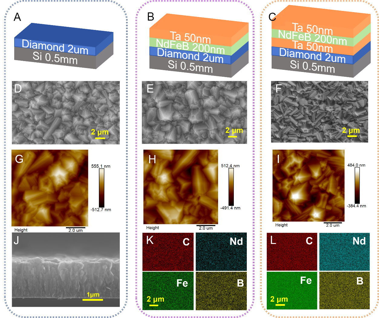
Figure 2. Morphology and elemental analysis characterization of diamond/NdFeB composite films. (A-C) Schematic diagrams of film growth for SD, SDNT2 and SDTNT2 samples, (D-F) Surface SEM of the corresponding samples, (G-I) AFM of the corresponding samples, (J) Cross-sectional SEM of the SD sample, (K and L) EDS elemental analysis of SDNT2 and SDTNT2 samples. SD: Si/diamond; SDNT: Si/diamond/NFB/Ta; SDTNT: Si/diamond/Ta/NFB/Ta; SEM: scanning electron microscope; AFM: atomic force microscope; EDS: energy-dispersive X-ray spectroscopy.
Magnetic and electrical properties of the composite films
To investigate the magnetic properties of the composite films, M-H hysteresis loops of the samples were measured at room temperature, as shown in Figure 1D-F. The hysteresis loop of the SD sample [Figure 1D] is a straight line passing through the origin, exhibiting diamagnetic behavior, which confirms that diamond itself does not contribute to ferromagnetism. The SDNT2 and SDNT4 samples display typical hysteresis loops for soft-magnetic materials, as represented in Figure 1E, with a significantly reduced coercivity (Hc) [Supplementary Figure 3] compared to bulk NdFeB. This ultra-low Hc [Supplementary Table 2] indicates that NdFeB exists in an amorphous state instead of a well-crystallized phase. The SDTNT2 sample [Figure 1F] possesses an extremely high Hc close to that of bulk NdFeB [Supplementary Table 2], indicating that the introduction of the Ta barrier layer effectively suppresses the direct atomic diffusion across the interface and weakens the interfacial coupling between the magnetic layer and the dielectric layer. The small lattice mismatch between the Ta and NdFeB planes promotes a high-quality epitaxial growth of NdFeB. When NdFeB is deposited on the Ta surface, columnar grains and out-of-plane texture form preferentially, leading to an excellent perpendicular magnetic anisotropy and promoting the formation of well-defined interfaces[40]. As a result, NdFeB experiences good crystalline growth. The amorphization-induced gradient interface effectively reduces the impedance mismatch and thus enhances the penetration of incident waves.
In SDNT2 and SDNT4 samples, the higher in-plane saturation magnetization originates from both magnetocrystalline and shape anisotropies. Notably, as the NdFeB thickness increases, the in-plane Ms increases, which can be attributed to the increased magnetic volume fraction; in contrast, the out-of-plane Ms decreases with increasing thickness, which is mainly due to the degradation of perpendicular magnetic anisotropy and the loss of c-axis out-of-plane texture in thicker films. These contrasting trends suggest a thickness-dependent anisotropic evolution: the in-plane magnetization is dominated by the volume effect, while the out-of-plane magnetization is governed by texture degradation. During the growth and subsequent annealing of the NdFeB film, the Ta layer acts as a transition metal interlayer that ensures favorable thermal expansion matching. Without this Ta layer, carbon diffusion into NdFeB suppresses its crystallization kinetics, disrupts long-range crystalline order, and thus prevents the formation of a crystalline structure, leading to a soft magnetic state[41,49]. This soft magnetic behavior is advantageous for optimizing the impedance matching of the composite films.
The electrical properties of the materials were characterized using a PPMS. Figure 1G-I represents the variation of Hall resistance (Rxy) with the applied magnetic field for the films with three types of interfacial structures. The carrier type is determined by the sign of the Hall coefficient RH, where RH < 0 corresponds to n-type (electron) conduction and RH > 0 to p-type (hole) conduction. The Hall coefficient is given by:
where t is the effective conducting thickness. Here, RH is extracted from the linear high-field region of the Rxy versus B curves, where the ordinary Hall effect (OHE) dominates and the anomalous Hall effect (AHE) contribution becomes saturated. The mobility is related to conductivity and Hall coefficient by:
where Rxx is determined from the Hall bar measurements. After substitution of the above relations, the mobility can be further simplified to:
The mobility μ represents the average drift velocity of carriers per unit electric field and is therefore an intrinsic transport parameter independent of the film thickness.
The negative slopes of all curves indicate n-type electronic conduction in the samples. For the SD film [Figure 1G], Rxy is nearly 10-4 Ω, with an overall linear behavior, representing an OHE. The Hall response is dominated by the intrinsic carrier transport in diamond. The calculated carrier mobility is μ = 2.9 cm2/(V·s), respectively. The low carrier mobility indicates that carriers can hardly respond to the alternating terahertz electric field. The SDTNT2 sample [Figure 1I] exhibits an AHE, with the curve showing a step-like saturation, which originates from the spontaneous magnetization of the NdFeB film[50]. The calculated carrier mobility is μ = 18.2 cm2/(V·s), respectively. The Ta interlayer effectively blocks the direct charge transfer at the interface, suppressing interfacial charge transfer and defect formation. The increased carrier mobility enables carrier drift under the alternating terahertz electromagnetic field, significantly enhancing the dielectric loss. The Hall curve of the composite film without an interlayer, SDNT2 [Figure 1H], shows features of a combined AHE and OHE. The coexistence of both the anomalous and ordinary Hall effects in the SDNT2 sample points to two independent conduction channels, consistent with the occurrence of interfacial diffusion and the accompanying formation of an sp2 carbon network. The carrier mobility extracted from the high-field region is μ = 54.5 cm2/(V·s), respectively. The enhanced mobility allows carriers to effectively follow the alternating terahertz electric field, leading to a strong dielectric loss. Meanwhile, the direct diamond/NdFeB interfacial coupling is expected to give rise to a compositionally graded transition layer at the interface, which may effectively alleviate the abrupt impedance contrast.
Microstructure analysis
The layered compositions and thicknesses of the diamond/NdFeB composite films with three distinct interfacial configurations are illustrated in Figure 2A-C. It is worth noting that all NdFeB-containing samples are capped with a Ta layer of approximately 50 nm in thickness, which serves as an oxidation protection layer. The surface morphology and roughness of the composite films were investigated using SEM and AFM, as shown in Figure 2D-I. The surface SEM of the SD sample [Figure 2D] reveals a dense surface with clear grain boundaries. The corresponding AFM [Figure 2G] further quantifies its surface roughness, showing the highest values among the samples (Ra = 114 nm, Rmax = 982 nm) [Supplementary Table 3]. The cross-sectional SEM [Figure 2J] indicates that the diamond layer exhibits a columnar grain structure, growing vertically along the substrate without the secondary phase. The grain size of diamond is approximately 1.5 μm. Its relatively high surface roughness stems from the significant difference in growth rates among different crystal planes, resulting in the morphological features of large grain protrusions and grain boundary depressions. With the protrusion of grain tips and longitudinal extension of grain boundaries, the surface roughness accumulates linearly with the film thickness, which is closely associated with the anisotropy of materials[51]. Although surface roughness introduces additional scattering losses, its contribution in the TEMW band is significantly smaller than the shielding effect caused by surface reflection. Consequently, the majority of TEMW is reflected back into free space, resulting in an overall extremely low absorption for the SD sample.
The growth schematic of the SDNT2 sample [Figure 2B] illustrates the direct contact between diamond and NdFeB layers. Its surface SEM [Figure 2E] displays a morphology typical of diamond. AFM analysis [Figure 2H] shows a surface roughness of Ra = 89.7 nm [Supplementary Table 3], which is lower than that of the pure diamond film. For the SDTNT2, a 50 nm thick Ta layer was deposited as an interlayer during film growth to prevent direct contact between the diamond and NdFeB. The surface SEM [Figure 2F] indicates that the surface remains relatively rough. The AFM result [Figure 2I] demonstrates a roughness nearly identical to that of the sample without an interlayer (Ra = 89.4 nm) [Supplementary Table 3]. Meanwhile, elemental analysis via EDS [Figure 2K and L] confirms that all detected elements are the target components of the samples, with uniform element distribution and no obvious aggregation. This indicates that NdFeB does not exhibit agglomerated growth. The uniform distribution of Ta has been confirmed by the EDS mapping results presented in Supplementary Figure 4. The enhancement in absorption performance, therefore, does not depend on the absolute value of surface roughness, but rather on factors such as the compositional gradient at the interface, defect density, and synergistic interfacial effects.
TEMW absorption performance
Interfacial structure engineering of the composite effectively optimizes the electromagnetic parameters and promotes impedance matching. The synergistic realization of a favorable impedance matching and a sufficient attenuation capability enables highly efficient EMW absorption. Figure 3 presents the electromagnetic absorption and shielding performance of the diamond/NdFeB composite films in the 170-220 GHz band. The S parameters of the composite thin films in the frequency range of 170-220 GHz were measured by VNA in reflection and transmission modes [Supplementary Figure 5], respectively, with the results presented in Figure 3A and B. The SD sample exhibits the highest S11 magnitude and the lowest S21 magnitude, indicating a strong reflection and a weak transmission of TEMW. After introducing the NdFeB magnetic layer, the S11 magnitude of the composite films decreases, indicating that the magnetic layer effectively improves the impedance matching and suppresses the surface reflection. Concurrently, the S21 magnitude increases, reflecting enhanced wave penetration, which allows more energy to enter the material and participate in loss mechanisms.
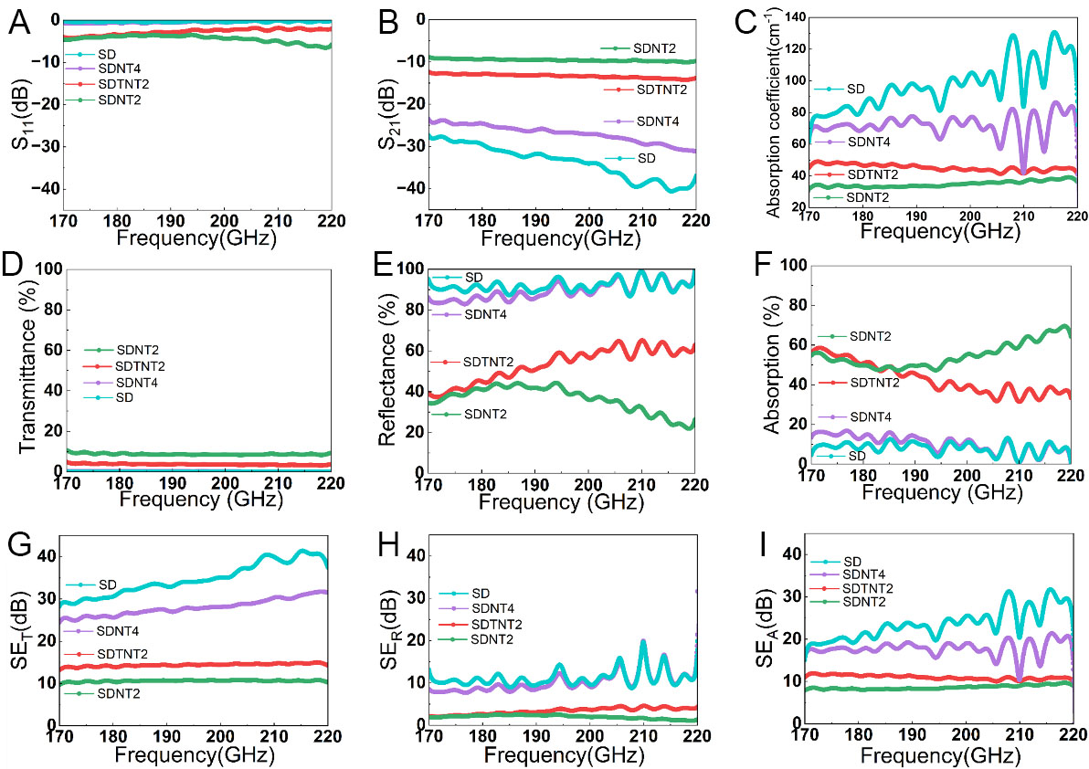
Figure 3. Electromagnetic wave absorption properties of diamond/NdFeB composite films in the frequency range of 170-220 GHz. (A) S11 parameter, (B) S21 parameter, (C) absorption coefficient, (D) transmittance, (E) reflectance, (F) absorptivity, (G) total EMI SE, (H) reflection EMI SE, (I) absorption EMI SE. SD: Si/diamond; SDNT: Si/diamond/NFB/Ta; SDTNT: Si/diamond/Ta/NFB/Ta; EMI: electromagnetic interference; SE: shielding effectiveness.
The S parameters were first converted into linear magnitudes using
The transmissivity (T) and reflectivity (R) were evaluated according to
respectively. where ETs(ω) and ETr(ω) refer to the electric field amplitude of the sample and reference in transmission mode, respectively. ERs(ω) and ERr(ω) refer to the amplitude of the sample and reference in reflection mode, respectively[52].
The absorptivity (A) was obtained as follows,
The absorption coefficient (α) was calculated from the measured transmittance (T) and reflectance (R) using the modified Beer-Lambert law, as given in
where d represents the total thickness of the composite film sample. The term T/(1 - R) represents the fraction of the incident wave that enters the sample and is subsequently transmitted, assuming that multiple internal reflections are negligible and that the sample thickness is sufficiently small compared to the coherence length of the terahertz wave. Notably, the use of the total film thickness in the calculation is physically appropriate, as the electromagnetic wave propagates and attenuates through the entire film stack during the transmission/reflection measurement, rather than through a single sublayer alone. It should be noted that the absorption coefficient α reported in this work is defined as the absorption coefficient of the entire composite film stack, rather than the intrinsic absorption coefficient of any individual layer.
The absorption coefficient curves in Figure 3C indicate that the SD sample possesses the highest absorption coefficient, with an overall increasing trend as the frequency increases. However, the SD sample achieves an extremely low actual electromagnetic wave absorptivity. The absorption coefficient reflects the loss capability of the samples, while the actual absorption performance is jointly determined by the impedance matching and the intrinsic loss. Therefore, although the SDNT2 sample has the lowest absorption coefficient, its excellent impedance matching results in a much higher actual absorptivity than that of SD sample, confirming the critical role of the magnetic interfacial coupling in regulating absorption performance of the composite films.
The transmissivity, reflectivity, and absorptivity were further calculated [Figure 3D-F]. The SD sample exhibits strong reflection and negligible absorption in the 170-220 GHz band. In contrast to the SD sample, the SDNT2 sample without an interlayer, achieves a transmittance of 10%, a reflectance below 45%, and an absorptivity exceeding 47%, with a maximum value of 70%. The absorption characteristics of SDNT2 are mainly derived from two aspects: one is the interfacial polarization induced by the band structure difference between diamond and NdFeB, and the other is the high-density defects formed after interfacial compositing. These defects act as polarization centers, generating a high-frequency polarization relaxation. The above two mechanisms jointly contribute to the dielectric loss of the material. Additionally, the amorphous NdFeB layer considerably reduces the magnetocrystalline anisotropy of the material, endowing NdFeB with excellent soft-magnetic properties and thus effectively optimizing the impedance matching of the composite thin films.
In contrast, the SDNT4 sample shows a reflectance increased to above 80% and an absorptivity significantly reduced to below 20%, which is much lower than that of SDNT2 sample. Its absorption and reflection performances are instead similar to those of the SD sample. A 200 nm-thick NdFeB layer is sufficient to fully develop the interface effect while avoiding defect dilution. For the sample with a 400 nm-thick magnetic layer, the increase of the thickness reduces the relative interface proportion of the sample, and deteriorates the impedance matching characteristics, eventually resulting in a rise in reflectance and a decline in absorptivity. For the SDTNT2 sample, the transmittance remains below 5% with negligible frequency dependence, while the reflectance exhibits an increasing trend with frequency, reaching a maximum of 65%. The absorptivity ranges from 30% to 60% overall and decreases with rising frequency indicating that the combination of indirect interfacial coupling and hard magnetic materials is not conducive to achieving broadband absorption performance. The Ta interlayer between diamond and NdFeB effectively inhibits the interfacial coupling effect. Nevertheless, the two new interfaces (diamond/Ta and Ta/NdFeB) introduced by the interlayer also contribute to improved impedance matching and introduce additional interfacial defects, leading to a strong dielectric relaxation. It should be noted that this comparison involves two coupled effects, namely the removal of the direct interface and the introduction of new Ta-related interfaces, and the current design does not fully isolate them. Nevertheless, the dominant role of direct diamond/NdFeB interfacial coupling is strongly supported by the superior absorption performance and structural evidence observed in SDNT2. As a result, its absorption is still superior to that of the SD sample, but the lack of direct contact coupling at the interface limits the room for improvement in absorptivity.
Figure 3G-I presents the shielding effectiveness (SE) parameters of the four sample groups. SE including SET, SEA, and SER was evaluated by
where SET refers to the total electromagnetic interference (EMI) shielding effectiveness. SEA and SER are the contributions of absorption and reflection[53].
Among them, the SD sample exhibits the highest values across all three parameters, indicating that the material itself possesses an excellent dielectric loss capability while also having an extremely strong reflective shielding performance. However, its excessively strong reflectivity prevents the effective utilization of the material’s absorption loss potential, ultimately resulting in a reflection-dominant shielding mechanism. It is a typical reflection-type shielding material, which is prone to causing secondary electromagnetic pollution. Due to the improper thickness of the magnetic layer, the SDNT4 sample fails to achieve an optimal impedance matching, and its shielding performance is similarly dominated by reflection. In contrast, the SDNT2 and SDTNT2 samples have appropriate impedance matching with free space, where the reflective shielding effectiveness of SDNT2 and SDTNT2 is lower than that of the other samples, making absorption the dominant shielding mechanism. They exhibit typical absorption-dominant shielding characteristics, resulting in significantly reduced secondary electromagnetic pollution. Nevertheless, the SDTNT2 sample still retains a small amount of reflective shielding capability in the high-frequency band, which leads to a decrease in its absorptivity at high frequencies, making its performance inferior to that of the SDNT2 sample.
Analysis of dielectric parameters
The spectral characteristics of the dielectric properties of the composite thin films in the frequency range of 170-220 GHz were characterized using a VNA [Figure 4], revealing the regulatory mechanism of interfacial structure and magnetic layer thickness on the dielectric properties and dielectric loss of the system. According to the Debye relaxation theory, for the polarization-relaxation process where the contribution of electrical conductivity can be neglected, the complex permittivity [Figure 4A and B] follows Equations 12 and 13[54],
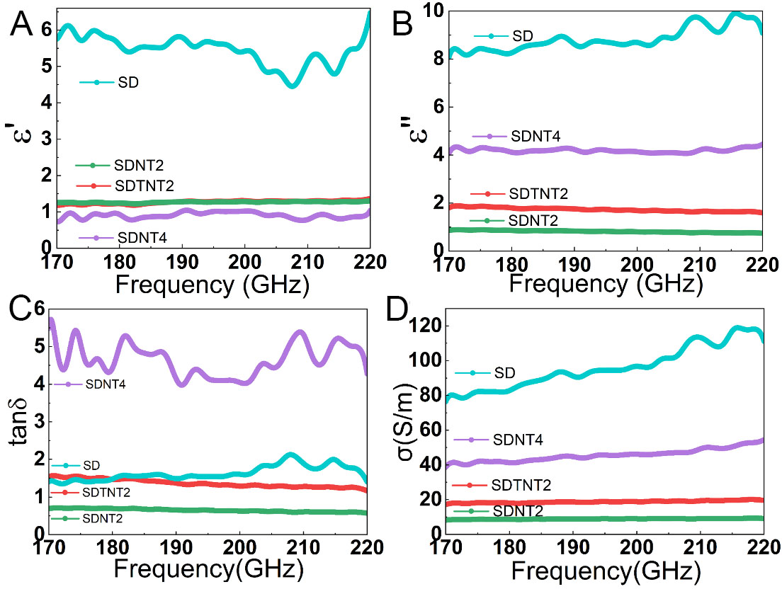
Figure 4. Dielectric properties of diamond/NdFeB composite thin films in the frequency range of 170-220 GHz: (A) real part of dielectric constant; (B) imaginary part of dielectric constant; (C) loss tangent, (D) electrical conductivity.
where ω = 2πf is the angular frequency, ε∞ is the dielectric constant at the high-frequency limit, εs is the static dielectric constant, and τ is the polarization relaxation time.
The dielectric loss tangent [Equation 14] is generally adopted to evaluate the dielectric loss capability of materials [Figure 4C][55].
The formula for the AC electrical conductivity of the material [Equation 15] can be derived based on the free electron theory,
where σ represents the AC electrical conductivity and ε0 denotes the permittivity of vacuum[56]. The AC conductivity at THz frequencies is directly extracted from the complex permittivity spectra, which reflects the combined contributions of localized polarization relaxation.
As shown in Figure 4A and B, the SD sample maintains the highest dielectric parameters across the entire 170-220 GHz band. However, its AC electrical conductivity [Figure 4D] is nearly one order of magnitude larger than that of the SDNT2 sample. The excessively high conductivity gives rise to severe impedance mismatch under the external electromagnetic field, resulting in a remarkable degradation of the wave absorption performance. Consequently, despite its high dielectric values, the actual absorption rate is extremely low, ultimately manifesting as reflection-dominant shielding characteristic. With the introduction of the NdFeB magnetic layer, the dielectric parameters of the composite films decrease notably and show minimal frequency dependence overall. The SDNT2 sample, benefiting from the electromagnetic interfacial coupling effect, effectively reduces the AC electrical conductivity σ. While suppressing surface reflection, it simultaneously achieves the synergistic optimization of loss capability and impedance matching by balancing the real part ε' and imaginary part ε'' of the complex permittivity. Analysis on the real part of the complex refractive index of the composite films [Supplementary Figure 6A] shows that the refractive index of the SDNT2 sample is 1.2 and slightly higher than that of free space, suggesting its superior impedance matching performance that favors the effective penetration of electromagnetic waves into the film. A stable imaginary part of the complex refractive index over a wide bandwidth suggests the potential for a broadband loss response [Supplementary Figure 6B]. Thus, the dielectric loss enhancement in SDNT2 reflects the effective loss under optimized impedance matching, rather than simply arising from permittivity values. This distinction is critical for understanding the present loss mechanism.
In contrast, the Ta interlayer in the SDTNT2 sample effectively blocks the direct interfacial contact between diamond and NdFeB, allowing both components to retain their intrinsic electromagnetic properties. The loss mechanism in this system is dominated by the interfacial polarization at the diamond/Ta and Ta/NdFeB interfaces, as well as defect-induced dipole polarization. Restricted by the narrow relaxation frequency range of these polarization processes, the tan δ [Figure 4C] gradually decreases with increasing frequency, accompanied by a significant decline in the terahertz absorption performance of the sample. For the SDNT4 sample, when the thickness of the NdFeB layer is increased to 400 nm, the excessively thick magnetic layer leads to a remarkable rise in the imaginary part of permittivity and electrical conductivity, thus deteriorating the impedance matching between the film and free space. Consequently, even though the contribution of intrinsic loss cannot be neglected, the inefficient incidence of electromagnetic waves results in much lower overall absorption compared with SDNT2. These results demonstrate that both the interfacial structure and the thickness of the magnetic layer are key parameters for regulating the dielectric and terahertz absorption properties of the diamond/NdFeB composite system. Achieving an optimal absorption performance in the terahertz range requires a delicate balance between enhancing the dielectric loss and maintaining the favorable impedance matching.
Based on Debye’s theory, the relationship between the real and imaginary parts of the permittivity during the electric dipole polarization-relaxation process can be given by
The curve plotted based on the relationship between the real part (ε') and the imaginary part (ε") of the complex permittivity is known as the Cole-Cole plot, as shown in Figure 5. In these plots, each semicircular arc corresponds to a Debye-type dipolar polarization-relaxation process. A larger arc radius indicates higher relaxation strength and stronger dielectric loss [Figure 5A], while a greater number of arcs reflects a richer variety of polarization mechanisms[57].
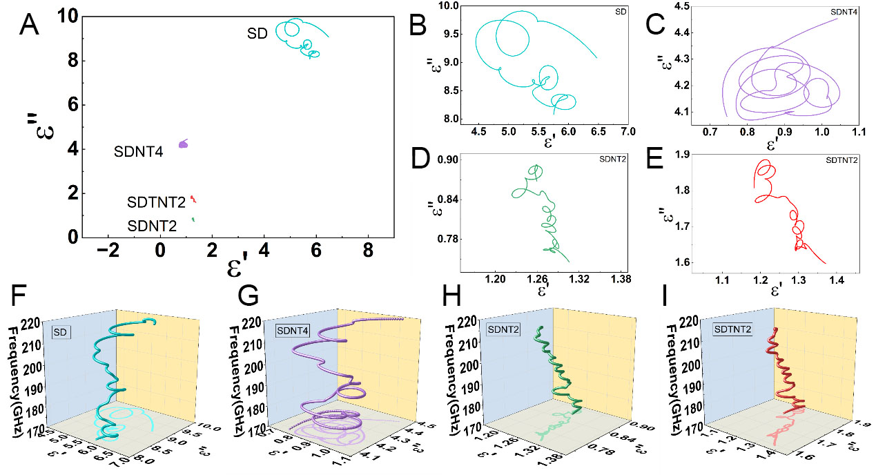
Figure 5. Cole-Cole plots of diamond/NdFeB composite films in the 170-220 GHz range. (A) overall plot, (B and F) 2D and 3D Cole-Cole plots for the SD sample, respectively; (C and G) 2D and 3D Cole-Cole plots for the SDNT4 sample, respectively; (D and H) 2D and 3D Cole-Cole plots for the SDNT2 sample, respectively; (E and I) 2D and 3D Cole-Cole plots for the SDTNT2 sample, respectively. SD: Si/diamond; SDNT: Si/diamond/NFB/Ta; SDTNT: Si/diamond/Ta/NFB/Ta.
Figure 5B and F reveals that multiple arcs with large radii appear in the SD sample, while several large nested arcs can be observed in the SDNT4 sample [Figure 5C and 5G], both of which correspond to multiple dielectric relaxation processes. Nevertheless, both samples demonstrate remarkably high reflectivity, which affirms the critical tenet that impedance matching takes precedence over intrinsic dielectric loss for electromagnetic wave-absorbing materials. For the SDNT4 sample, despite its high dielectric relaxation strength, the excessive thickness of the magnetic layer degrades impedance matching, leading to increased reflectance, resulting in an actual absorption rate of less than 20%. This result further verifies the critical role of optimizing the magnetic layer thickness for achieving a high-efficiency wave absorption performance. In Figure 5D and H, the SDNT2 sample shows multiple small-radius arcs. The strong interfacial magnetoelectric coupling formed between diamond and NdFeB gives rise to intense interfacial polarization and defect-induced polarization relaxation, thereby tuning the dielectric loss to an optimal level. A similar arc pattern is observed for the SDTNT2 sample in Figure 5E and I, consistent with its comparable loss performance.
According to the Debye relaxation theory, each polarization process is characterized by a relaxation time τ and a characteristic frequency fr =1/(2πτ), where arcs at higher frequencies correspond to shorter relaxation times. Based on the Debye relaxation theory, the multiple semicircular arcs in the Cole-Cole plot of the SDNT2 sample are suggestive of several polarization relaxation processes. The high-frequency semicircular arc is mainly associated with defect dipole relaxation. These defect dipoles, such as dangling bonds and atomic misalignments generated during amorphization, are light and respond rapidly with short relaxation times, thereby contributing to the high-frequency region. The mid-frequency arc likely corresponds to dipole orientation polarization, originating from the reorientation of permanent dipole moments of molecular groups under the alternating electric field. The low-frequency arc is possibly related to interfacial polarization, involving space-charge accumulation and redistribution at the diamond/NdFeB interface, a process characterized by longer relaxation times and lower characteristic frequencies. These multiple overlapping relaxation processes collectively account for the broadband dielectric loss observed in the SDNT2 sample[58,59].
Compared with other studies on terahertz absorbing materials [Supplementary Table 4], this work does not pursue the highest absorptivity, but rather demonstrates a conceptual shift, transforming diamond into an efficient terahertz absorber through interfacial engineering with NdFeB. The electromagnetic loss of the SDNT2 sample in the terahertz (170-220 GHz) band mainly originates from the synergistic effects of interfacial polarization relaxation and dipole polarization (as illustrated in Figure 6). Based on the well-established semiconductor physics for metal-semiconductor contacts and the observed structural features at the diamond/NdFeB interface, it is reasonable to infer that charge redistribution occurs at the interface, which would induce downward band bending in diamond, forming an intrinsic interfacial dipole layer and a space-charge region. This is expected to promote carrier separation and strengthen interfacial polarization, thereby contributing to the enhanced dielectric loss. Lattice mismatch and the notable electronegativity difference introduce tensile/compressive strains and charge transfer, constructing an intrinsic interfacial dipole layer, exacerbating a band bending and strengthening an interfacial polarization. Structural characterization indicates that the NdFeB layer undergoes severe structural disordering and amorphization, accompanied by the formation of sp²-hybridized carbon species. This diffusion destroys the long-range crystalline order of the Nd2Fe14B phase. The amorphization generates a high density of structural defects (e.g., dangling bonds, atomic misalignment) at the interface. Interfacial defects serve as additional polarization centers, which undergo a directional reorientation under terahertz electromagnetic field and thus give rise to defect dipole relaxation. These interfacial effects collectively regulate the local electronic structure, providing core mechanistic support for optimizing terahertz absorption performance. Finally, the SDNT2 sample achieves an efficient THz absorption through the direct interfacial coupling, which effectively balances dielectric polarization and impedance matching. These results provide direct experimental evidence and theoretical guidance for optimizing the interfacial structure design and magnetic layer thickness in diamond-based TEMW absorbing materials.
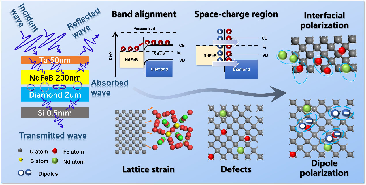
Figure 6. Schematic illustrations for the TEMW absorption mechanism of SDNT2 sample. TEMW: Terahertz electromagnetic waves; CB: conduction band; VB: valence band; EF: Fermi level; SDNT: Si/diamond/NFB/Ta.
CONCLUSIONS
In this study, diamond/NdFeB composite films with different interfacial structures and magnetic layer thicknesses were fabricated, and their TEMW absorption performance in the 170-220 GHz band was measured. The results show that among the three thicknesses investigated (0, 200, and 400 nm), the sample with a 200 nm-thick NdFeB layer and no Ta interlayer exhibits the highest TEMW absorption performance, with the average absorption rate increasing from approximately 10% (pure diamond) to over 47% (up to 70%) in the 170-220 GHz band. An intermediate thickness is therefore favorable for balancing interfacial polarization and impedance matching. Interfacial magnetoelectric coupling induced by direct contact softens NdFeB coercivity, reduces conductivity to optimize impedance matching, suppresses reflection, and enhances dielectric loss via inducing multiple types of polarization relaxation processes for the synergistic enhancement of electromagnetic loss. Within the thickness range examined in this work, the 200 nm NdFeB layer demonstrated better absorption performance, likely due to a higher effective defect density and better impedance matching, while the 400 nm layer exhibited inferior performance associated with defect dilution and impedance degradation. Furthermore, while the present results indicate that direct interfacial coupling is the dominant mechanism, the experimental design could not fully separate the effects of removing the direct interface and introducing new Ta-related interfaces. Future work incorporating more refined interfacial architectures or alternative interlayer materials would be valuable to further disentangle the respective contributions of direct interfacial coupling and Ta-related interface effects. Through interfacial engineering with NdFeB and concurrent magnetic modulation, this work enables diamond to function as a terahertz absorber, and elucidates the regulatory roles of interfacial structure and magnetic layer thickness, thereby offering both experimental and theoretical guidance for the rational design of high-performance diamond-based TEMW absorbers.
DECLARATIONS
Authors’ contributions
Writing - original draft: Wang, J.
Visualization: Wang, J.
Methodology: Wang, J.; Ma, L.
Investigation: Wang, J.
Formal analysis: Wang, J.; Ma, L.; Qiu, W.; Li, B.; Li, C.; Li, D.; Bai, C.; Lv, Z.; Jiang, Z.; Zhao, R.; Qi, F.; Huang, N.; Liu, W.; Ma, S.
Data curation: Wang, J.
Writing - review & editing: Zhang, H.; Ma, L.; Ma, S.; Zhang, Z.
Supervision: Ma, L.; Ma, S.; Zhang, Z.
Funding acquisition: Ma, L.; Li, D.; Bai, C.; Ma, S.
Conceptualization: Ma, L.; Ma, S.
Resources: Ma, S.
Project administration: Ma, S.
Availability of data and materials
The data supporting the findings of this study are available within this Article and its Supplementary Materials. Further data are available from the corresponding authors upon request.
AI and AI-assisted tools statement
Not applicable.
Financial support and sponsorship
This work was supported by the National Key R&D Program of China with No. 2023YFF0718303.
Conflicts of interest
Lv, Z.; Jiang, Z.; Zhao, R. are affiliated with CETC Ceyear Technologies Co., Ltd., while the other authors have declared that they have no conflicts of interest.
Ethical approval and consent to participate
Not applicable.
Consent for publication
Not applicable.
Copyright
© The Author(s) 2026.
Supplementary Materials
REFERENCES
1. Yang, Y.; Yamagami, Y.; Yu, X.; et al. Terahertz topological photonics for on-chip communication. Nat Photonics. 2020, 14, 446-51.
2. Xue, Q.; Ji, C.; Ma, S.; et al. A survey of beam management for mmWave and THz communications towards 6G. IEEE Commun. Surv. Tutorials. 2024, 26, 1520-59.
3. Jiang, W.; Zhou, Q.; He, J.; et al. Terahertz communications and sensing for 6G and beyond: A comprehensive review. IEEE Commun. Surv. Tutorials. 2024, 26, 2326-81.
4. Polese, M.; Cantos-roman, X.; Singh, A.; et al. Coexistence and spectrum sharing above 100 GHz. Proc. IEEE. 2023, 111, 928-54.
5. Huang, Y.; Shen, Y.; Wang, J. From terahertz imaging to terahertz wireless communications. Engineering. 2023, 22, 106-24.
6. Ahmadivand, A.; Gerislioglu, B.; Ahuja, R.; Kumar, Mishra. Y. Terahertz plasmonics: the rise of toroidal metadevices towards immunobiosensings. Mater Today. 2020, 32, 108-30.
7. Malevich, Y.; Ergoktas, M. S.; Bakan, G.; Steiner, P.; Kocabas, C. Video-speed graphene modulator arrays for terahertz imaging applications. ACS Photonics. 2020, 7, 2374-80.
8. Bao, Y.; Yin, Q.; Liu, C.; et al. Conformal sensors enhanced by flexible terahertz microstructures. TrACTrend Anal Chem. 2026, 194, 118545.
9. Yu, E. S.; Lee, S. H.; Lee, G.; et al. Nanoscale terahertz monitoring on multiphase dynamic assembly of nanoparticles under aqueous environment. Adv Sci. 2021, 8, 2004826.
10. Iqbal, A.; Hassan, T.; Naqvi, S. M.; Gogotsi, Y.; Koo, C. M. MXenes for multispectral electromagnetic shielding. Nat Rev Electr Eng. 2024, 1, 180-98.
11. Li, S.; Xu, S.; Pan, K.; Du, J.; Qiu, J. Ultra-thin broadband terahertz absorption and electromagnetic shielding properties of MXene/rGO composite film. Carbon. 2022, 194, 127-39.
12. Sharma, S.; Parne, S. R.; Panda, S. S. S.; Gandi, S. Progress in microwave absorbing materials: a critical review. Adv Colloid Interface Sci. 2024, 327, 103143.
13. Peng, H.; Zhang, D.; Xie, Z.; Lu, S.; Liu, Y.; Liang, F. Recent advances in structural design of carbon/magnetic composites and their electromagnetic wave absorption applications. Small. 2025, 21, 2408570.
14. Chen, C.; Chai, M.; Jin, M.; He, T. Terahertz metamaterial absorbers. Adv Mater Technol. 2022, 7, 2101171.
15. Xu, W.; Xie, L.; Ying, Y. Tunable transparent terahertz absorber for sensing and radiation warming. Carbon. 2023, 214, 118376.
16. Pham, P. H. Q.; Zhang, W.; Quach, N. V.; et al. Broadband impedance match to two-dimensional materials in the terahertz domain. Nat Commun. 2017, 8, 2233.
17. Chen, H.; Lin, H.; Wang, X.; et al. Harmonizing material quantity and terahertz wave interference shielding efficiency with metallic borophene nanosheets. Nat Commun. , 16, 5739.
18. Yu, P.; Besteiro, L. V.; Huang, Y.; et al. Broadband metamaterial absorbers. Adv Opt Mater. 2019, 7, 1800995.
19. Wang, B. X.; Xu, C.; Duan, G.; Xu, W.; Pi, F. Review of broadband metamaterial absorbers: from principles, design strategies, and tunable properties to functional applications. Adv Funct Mater. 2023, 33, 2213818.
20. Baah, M.; Paddubskaya, A.; Novitsky, A.; et al. All-graphene perfect broadband THz absorber. Carbon. 2021, 185, 709-16.
21. Iqbal, A.; Hong, J.; Ko, T. Y.; Koo, C. M. Improving oxidation stability of 2D MXenes: synthesis, storage media, and conditions. Nano Converg. 2021, 8, 9.
22. Zhao, T.; Xie, P.; Wan, H.; et al. Ultrathin MXene assemblies approach the intrinsic absorption limit in the 0.5-10 THz band. Nat Photonics. 2023, 17, 622-8.
23. Guo, Y.; Chen, Z.; Jin, Z.; et al. Dynamically controllable terahertz electromagnetic interference shielding by small polaron responses in Dirac semimetal PdTe2 thin films. Adv Funct Mater. 2024, 34, 2407749.
24. Zhang, L.; Liu, W.; Cencillo-Abad, P.; Wang, Q.; Huang, X.; Leng, Y. A tunable broadband polarization-independent metamaterial terahertz absorber based on VO2 and Dirac semimetal. Opt Commun. 2023, 542, 129602.
25. Ren, T.; Li, C. VO2-based temperature-adaptive radiative materials towards real-world applications: A review. Appl Energy. 2025, 399, 126540.
26. Liang, L.; Gu, W.; Wu, Y.; et al. Heterointerface engineering in electromagnetic absorbers: new insights and opportunities. Adv Mater. 2022, 34, 2106195.
27. Zhao, T.; Wan, H.; Zhang, T.; Xiao, X. Mechanism of the terahertz wave-MXene interaction and surface/interface chemistry of MXene for terahertz absorption and shielding. Acc Chem Res. 2024, 57, 2184-93.
28. Li, J.; Yuan, X.; Sun, H.; Yao, Y.; Cao, Q.; Che, R. Interface engineering for next generation low-frequency electromagnetic wave absorption materials. Adv Funct Mater. 2026, 36, e77440.
29. Zhang, S.; Wen, F.; Zhai, M.; et al. Terahertz dynamic multiband perfect absorber with a digital coding graphene-diamond metasurface. Phys Rev Appl. 2024, 22, 024004.
30. Li, Y.; Yang, L.; Jiang, X.; et al. Diamond nanostructures at different dimensions: synthesis and applications. Adv Funct Mater. 2024, 34, 2314558.
31. Khabashesku, V.; Filonenko, V.; Bagramov, R.; Zibrov, I.; Anokhin, A. Nanoengineered polycrystalline diamond composites with advanced wear resistance and thermal stability. ACS Appl Mater Interfaces. 2021, 13, 59560-6.
32. Guo, Y.; Wang, D.; Wang, Z.; et al. Magnetic properties and dielectric properties of CoFeB/NdFeB composite films at Terahertz. Compos Commun. 2025, 53, 102242.
33. Mu, Z.; Xie, P.; Alshammari, A. S.; et al. Magnetic metal-based MOF composite materials: a multidimensional regulation strategy for microwave absorption properties. Adv Compos Hybrid Mater. 2024, 7, 171.
34. Cheng, C.; Sun, X.; He, X.; et al. Atomic and electronic properties of the metal/diamond (100) interfaces by first-principles calculations. Surf Interfaces. 2024, 52, 104916.
35. Lee, K. H.; Seong, W. K.; Ruoff, R. S. CVD diamond growth: Replacing the hot metallic filament with a hot graphite plate. Carbon. 2022, 187, 396-403.
36. Lv, F.; Wang, Y.; He, Q.; Lan, D.; Wu, G. High-entropy strategy-driven lattice distortion and electronic rearrangement in MOF-derived HEA/NC composites for balanced electromagnetic response and superior microwave attenuation. Adv Funct Mater. 2026, 36, e75416.
37. Zhao, B.; Yan, Z.; Du, Y.; et al. High-entropy enhanced microwave attenuation in titanate perovskites. Adv Mater. 2023, 35, 2210243.
38. Ku, Y.; Xu, K.; Yan, L.; et al. Revealing the atomic mechanism of diamond-iron interfacial reaction. Carbon Energy. 2024, 6, e440.
39. Carvalho, T.; Simão, R.; Archanjo, B.; Araújo, J.; Pereira, K. X.; Barthem, V. S. The fundamental role of Ta diffusion on the high coercivity of Ta/SmCo5/Ta and Ta/Sm2Co17/Ta films. J Alloys Compd. 2024, 990, 174414.
40. Ye, Z.; Zhao, X.; Liu, W.; et al. Enhancement of perpendicular magnetic anisotropy and formation of interface in Nd-Dy-Fe-Co-B thick film with Ta spacer layer. Surf Interfaces. 2023, 37, 102697.
41. Zeng, C.; Chen, S.; Feng, Q.; et al. Significant effects of residual carbon on the grain boundary diffusion of Nd-Fe-B magnets. J Alloys Compd. 2026, 1065, 188137.
42. Liang, J.; Gao, C.; Zhang, L.; et al. Studies on distribution of element contents in transient layer at interface between boron-doped diamond film electrode and tantalum substrate. Appl Surf Sci. 2011, 257, 6063-7.
43. Wang, P.; Guo, Z.; Sun, Z.; Li, G.; Bi, J.; Qian, L. Carrier gradient core-double shell structure with heterojunction transition layer for significantly enhancing dielectric properties. Chem Eng J. 2024, 496, 153968.
44. Cuenca, J. A.; Thomas, E. L. H.; Mandal, S.; et al. Microwave permittivity of trace sp2 carbon impurities in sub-micron diamond powders. ACS Omega. 2018, 3, 2183-92.
45. Piazza, F.; Kelvin, Cruz.; Monthioux, M.; Puech, P.; Gerber, I. Raman evidence for the successful synthesis of diamane. Carbon. 2020, 169, 129-33.
46. Korepanov, V. I.; Hamaguchi, H.; Osawa, E.; et al. Carbon structure in nanodiamonds elucidated from Raman spectroscopy. Carbon. 2017, 121, 322-9.
47. Ding, X.; Lyu, L.; Wang, F.; et al. Novel ternary Co3O4/CeO2/CNTs composites for high-performance broadband electromagnetic wave absorption. J Alloys Compd. 2021, 864, 158141.
48. Qin, M.; Zhang, L.; Wu, H. Dielectric loss mechanism in electromagnetic wave absorbing materials. Adv Sci. 2022, 9, 2105553.
49. Sasaki, T.; Ohkubo, T.; Une, Y.; Kubo, H.; Sagawa, M.; Hono, K. Effect of carbon on the coercivity and microstructure in fine-grained Nd-Fe-B sintered magnet. Acta Mater. 2015, 84, 506-14.
50. Yomogita, T.; Kikuchi, N.; Okamoto, S.; et al. Detection of elemental magnetization reversal events in a micro-patterned Nd-Fe-B hot-deformed magnet. AIP Adv. 2019, 9, 125052.
51. Shi, Y.; Chen, Z.; Yang, H.; Xie, J.; Xu, J. Micro- to nano-scale topographical etching of diamond substrate via anisotropically atomic removal. Appl Surf Sci. 2024, 655, 159589.
52. Yang, P.; Dai, M.; Xiong, H.; et al. 3D nickel skeletons as ultrabroadband terahertz absorbers. Adv Elect Mater. 2021, 7, 2100626.
53. Wei, Y.; Bhuyan, P.; Kwon, S. J.; et al. Liquid metal grid patterned thin film devices toward absorption-dominant and strain-tunable electromagnetic interference shielding. Nano-Micro Lett. 2024, 16, 248.
54. Cheng, J.; Chen, Q.; Wang, H.; et al. Engineering dielectric genes in Debye relaxation model toward frequency-band-reliant electromagnetic responses. Adv Mater. 2026, 38, e21471.
55. Zhao, P.; Wang, H.; Cai, B.; et al. Electrospinning fabrication and ultra-wideband electromagnetic wave absorption properties of CeO2/N-doped carbon nanofibers. Nano Res. 2022, 15, 7788-96.
56. Micheli, D.; Apollo, C.; Pastore, R.; Marchetti, M. X-Band microwave characterization of carbon-based nanocomposite material, absorption capability comparison and RAS design simulation. Compos Sci Technol. 2010, 70, 400-9.
57. Dong, S.; Song, J.; Zhang, X.; et al. Strong contribution of in situ grown nanowires to enhance the thermostabilities and microwave absorption properties of porous graphene foams under different atmospheres. J Mater Chem C. 2017, 5, 11837-46.
58. Koral, C.; Marsico, M.; Mazaheri, Z.; et al. Enhanced relaxation dynamics in silver-doped chitosan nanocomposites: Probing the charge carrier dynamics and terahertz dielectric response. Mater Chem Phys. 2025, 344, 131137.
Cite This Article
 Open Access
How to Cite
Wang, J.; Zhang, H.; Ma, L.; Qiu, W.; Li, B.; Li, C.; Li, D.; Bai, C.; Lv, Z.; Jiang, Z.; Zhao, R.; Qi, F.; Huang, N.; Liu, W.; Ma, S.; Zhang, Z. Tuning terahertz wave absorption in diamond/NdFeB composite films via magnetic interfacial engineering. Microstructures 2026, 6, 139. https://dx.doi.org/10.20517/microstructures.2026.159
Download Citation
If you have the appropriate software installed, you can download article citation data to the citation manager of your choice. Simply select your manager software from the list below and click on download.
Export Citation File
Type of Import
Tips on Downloading Citation
Citation Manager File Format
Type of Import
Direct Import: When the Direct Import option is selected (the default state), a dialogue box will give you the option to Save or Open the downloaded citation data. Choosing Open will either launch your citation manager or give you a choice of applications with which to use the metadata. The Save option saves the file locally for later use.
Indirect Import: When the Indirect Import option is selected, the metadata is displayed and may be copied and pasted as needed.
About This Article
Copyright

Data & Comments
Data
0











Comments
Comments must be written in English. Spam, offensive content, impersonation, and private information will not be permitted. If any comment is reported and identified as inappropriate content by OAE staff, the comment will be removed without notice. If you have any queries or need any help, please contact us at [email protected].