


Microstructural origin of dual band emission and thermal dynamics in suspended silicon-on-insulator infrared sources
 0
0  ,
, Abstract
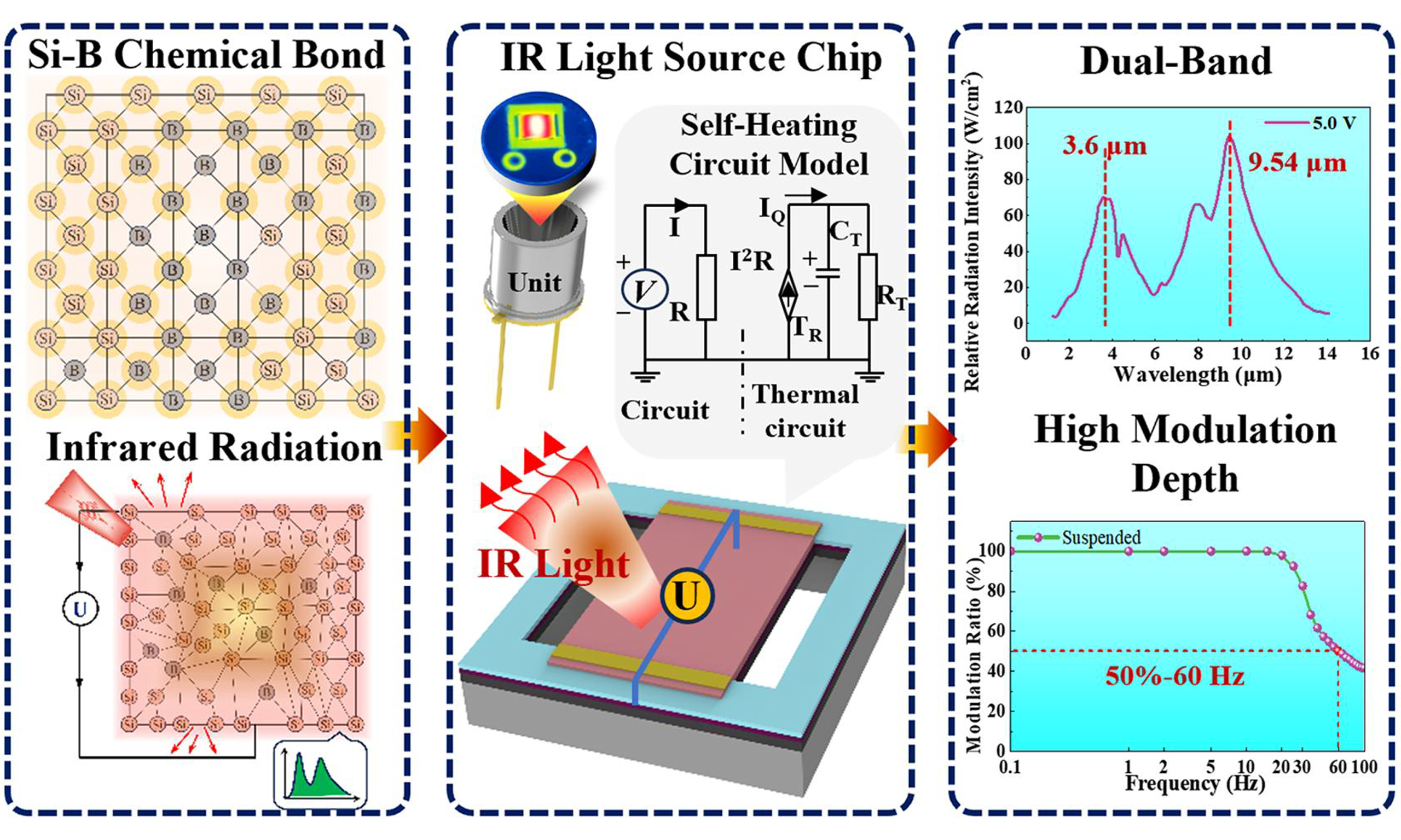
With the trend toward miniaturized and intelligent infrared systems, high-performance light source chips featuring a high modulation depth and rapid thermal response have emerged as key components for advancing interdisciplinary applications. In this study, a dual-band infrared source chip featuring a suspended membrane structure on a silicon-on-insulator substrate is reported. The suspended polysilicon emissive layer was prepared via high-concentration boron doping and micro-nano processing techniques. Relative to a closed membrane configuration, the suspended structure yields superior thermal and optical characteristics including a thermal response time of 36 ms to reach 450 °C, a modulation depth of 50% at 60 Hz, and dual-band emission centered at 3.6 and 9.54 μm. Structural-property correlation analysis reveals that the specific infrared emission signatures are intrinsically linked to the lattice microstructure. In particular, the 3.6 μm emission is attributed to the stretching vibrations of hydrogen-bridged bonds and Si-H bonds localized at oxygen vacancies within the surface SiO2 layer. In addition, the 9.54 μm peak originates from the coupling between the SiO2 network bending modes and the localized vibrational modes of Si-B bonds introduced by boron doping. Furthermore, the suspended membrane architecture plays a critical role in enhancing modulation performance by geometrically confining heat, thereby suppressing lateral thermal diffusion and reducing thermal capacitance. These insights establish a direct mapping between micro/nano-structural design and optoelectronic performance, offering a robust theoretical framework for developing high-efficiency infrared emitters for gas sensing and photodetection applications.
Keywords
INTRODUCTION
In recent years, infrared detection has become critical in fields such as optoelectronics[1], target identification[2], communications[3,4], and gas sensing[5-7]. The performance of these systems is dependent on their core component, the infrared light source, whose importance is amplified by the unique atmospheric windows and molecular absorption features in the mid- to long-wave infrared band. Therefore, a broad-spectrum source that seamlessly covers 2.5-14 μm is required for multiband convergence[8] and integrated systems as it directly affects the performance of modern infrared (IR) systems. Current IR sources include quantum cascade lasers (QCLs)[9-11], infrared light-emitting diodes (LEDs)[12-14], and thermal emitters[15-17]. Although QCLs offer high spectral density and single-mode operation, their cost and complexity limit their use in cost-sensitive applications[18]. In addition, infrared LEDs are restricted to narrow bands (< 5 μm) with low intensity[19], and thermal emitters, though cost-effective, suffer from high power consumption and slow responses[20]. micro-electromechanical systems (MEMS)-based emitters[21] have emerged as a promising system for overcoming these constraints to achieve compact, efficient, and high-performance infrared emission.
The performance of MEMS-based infrared thermal emitters is predominantly determined by the materials and structure of the infrared radiation layer, which directly influence the radiation temperature and modulation performance. In particular, thin-film infrared radiation layers are predominantly fabricated using metals and their oxides, carbon-based materials, and photonic crystal metamaterials[22]. Mele et al.[23] employed a sputtered molybdenum layer structured as a meander-shaped heater, achieving an infrared radiation temperature of up to 850 °C. In addition, Lee et al.[24] employed a platinum thin film as the heating layer to fabricate a meandering silicon beam filament, achieving an infrared radiation temperature of up to 1,000 °C. However, metallic heaters suffer from high power consumption and low resistivity, necessitating sophisticated patterning to achieve a viable resistance. Moreover, they exhibit low emissivity, a broad spectral bandwidth, and a lack of specific emission peaks in their infrared emission spectrum.
To address this issue, Lai et al.[25] employed super-aligned carbon nanotube (SACNT) thin-film material, attaining an infrared emissivity as high as 0.9 at a relatively low driving power. In addition, Wu et al.[26] fabricated a nanopatterned Pt/alumina bilayer cylindrical array photonic crystal emitter via MEMS microfabrication. They successfully achieved wavelength-tunable mid-infrared emission by introducing an insulating layer to suppress parasitic thermal diffusion. Likewise, Lochbaum et al.[20] integrated MEMS technology with a metamaterial perfect emitter (MPE), leveraging the surface plasmon polariton principle to achieve an exceptional emissivity of 0.99 at the emission peak of 3.96 μm. Although this approach resulted in high performance metrics, the maximum radiation temperature was limited to below 400 °C, primarily due to the thermal instability of carbon-based materials and metamaterial thin-film structures at elevated temperatures. Consequently, selecting heater materials that combine MEMS compatibility with high emissivity, low power consumption, and desirable radiative operating temperatures has emerged as a key research focus.
Currently, closed-type infrared thermal emitters dominate this field owing to their excellent thermal stability and long service life. Commercially available examples include the EMIRS200 from Axetris and the SIR series from Micro-Hybrid. Closed infrared sources have also been explored in the literature. Chang et al.[27] designed a closed infrared source featuring a multiturn U-shaped filament on a glass substrate. The device employed a composite thin-film structure of Cr/CrN/Pt/CrN/Cr as the heater, which enhanced its mechanical strength and operational stability. Although closed-type infrared thermal emitters exhibit excellent mechanical stability during heating, they lack a thermal isolation trench between the substrate and radiation layer, resulting in an inability to achieve effective heat transfer. Consequently, this structural limitation leads to high power consumption and a limited modulation-response speed[28]. To address these limitations, a suspended membrane structure based on a silicon-on-insulator (SOI) substrate is proposed in this study. The SOI substrate offers excellent compatibility with MEMS processes as the top silicon layer provides sufficient mechanical strength and reliability for the suspended structure under high-temperature thermal cycling. In addition, the buried oxide (SiO2) layer serves as an etch-stop layer for backside cavity etching and possesses superior electrical insulation properties. This enables effective thermal isolation, thereby contributing to reduced power consumption and an enhanced modulation capability and radiation temperature.
In this study, we demonstrate a dual-band MEMS infrared emitter constructed from a 6.6-μm-thick suspended polysilicon membrane, engineered for high-speed modulation and robust thermal emission. Boron-doped polysilicon was chosen as the active emissive layer owing to its superior complementary metal-oxide-semiconductor (CMOS) compatibility, tunable resistivity, and stability under high-temperature operation. This device uses a suspended architecture on an SOI substrate to enhance the thermal transient response, and this configuration effectively suppresses lateral thermal diffusion while substantially minimizing the thermal mass. The characterization results reveal a peak radiation temperature of 450 °C, thermal response time of 36 ms, and modulation depth of 50% at 60 Hz. Spectrally, the device demonstrates a broad average emissivity of 70% across the 2-14 μm band characterized by dual emission peaks. The proposed structure offers a promising solution for integrating high-performance portable gas sensors, IR identification units, and optoelectronic detection systems.
MATERIALS AND METHODS
Materials and fabrication
In this study, the fabrication of MEMS infrared chips commenced with 4-inch SOI wafers (OMedaSemi, Shanghai, China) featuring dimensionally uniform layers including a 4-μm-thick single-crystal silicon device layer, 1.5-μm-thick buried silicon dioxide (BOX) layer, and 400-μm-thick silicon substrate. The fabrication sequence is shown in Supplementary Figure 1. High-concentration boron ion diffusion (approximately
Characterization and measurement
A stylus profilometer (BRUKER Dektak XTL, USA) was employed to investigate the thickness of each layer on the surface of 4-inch wafers and characterize the nanoscale morphological properties of infrared-light-source chips. A focused ion beam scanning electron microscope (ZEISS Crossbeam 350, Germany) was used to characterize the layered structure of the suspended membrane and the elemental distribution across individual layers. The linewidth and pattern development after each photolithography step during the fabrication process and the final surface morphology of the polysilicon thin film on the chips were analyzed using a digital microscope (KEYENCE VHX-7000, Japan). All performance evaluations of the infrared light sources were conducted in a dark-field environment. A semiconductor device analyzer (Keysight B1500A, USA) and a digital source meter were used to measure the current-voltage (I-V) curves and thermal resistance characteristics of the light sources. In addition, an infrared thermal imager (FLIR T1050SC, USA) was used to determine the radiation temperature of the light sources under different input voltages and their thermal response under continuously modulated voltages. Square-wave signals with a 50% duty cycle were generated using a signal generator (RIGOL DG2102, China). The radiation results were converted into voltage signals using a spectral radiometer (SR5000, China) to investigate the light source response time and modulation depth. A Fourier transform infrared (FTIR) spectrometer equipped with an integrating sphere (Nicolet IS50, USA) was used to measure the emissivity of the light sources at 5 V. In addition, the radiation intensity characteristics and electro-optical conversion efficiency of the light sources under varying input voltages were characterized using a photometer (FPBEN-Enviro300, China). All infrared source samples with suspended and semi-closed membrane structures used in the characterization tests were fabricated using the same conditions except for the etching method.
RESULTS AND DISCUSSION
Design
Figure 1A shows the schematic of the proposed MEMS-based suspended membrane infrared-light-source chip. The proposed device is based on a microbridge structure and further developed into a polysilicon infrared-light-emitting film, which is suspended above an SOI substrate and only 0.5 μm thick. An SOI substrate was used because of its low thermal conductivity[29], which facilitates the upward propagation of thermal radiation to the suspended membrane. A 1.5-μm-thick SiO2 buried layer is located in the middle of this system, which can serve as a mask for the anisotropic dry etching of the bottom Si substrate, thereby simplifying the critical microfabrication release process. The top layer is a 4-μm-thick heavily boron-doped single-crystal silicon layer that can absorb and store the heat radiated downward from the polysilicon thin film, thereby achieving a self-heating effect. The heating layer of the device comprises a 0.5-μm-thick boron-doped polysilicon layer capped with thermally grown SiO2. This layer acts as a mask for boron ion implantation in polysilicon, eliminates the channeling effect[30] resulting from ion implantation, and prevents the oxidation of polysilicon films during high-temperature operation[31,32]. A 0.5-μm-thick SiO2 layer sandwiched between the heating element and SOI substrate provides simultaneous electrical and thermal isolation. For enhanced clarity and analysis, the three-dimensional schematic was sectioned along A-A plane, yielding the cross-sectional view presented in Figure 1B. It can be clearly seen that the device layer is suspended above the bottom Si substrate, with both lateral ends open to air cavities to form a structurally independent membrane configuration.
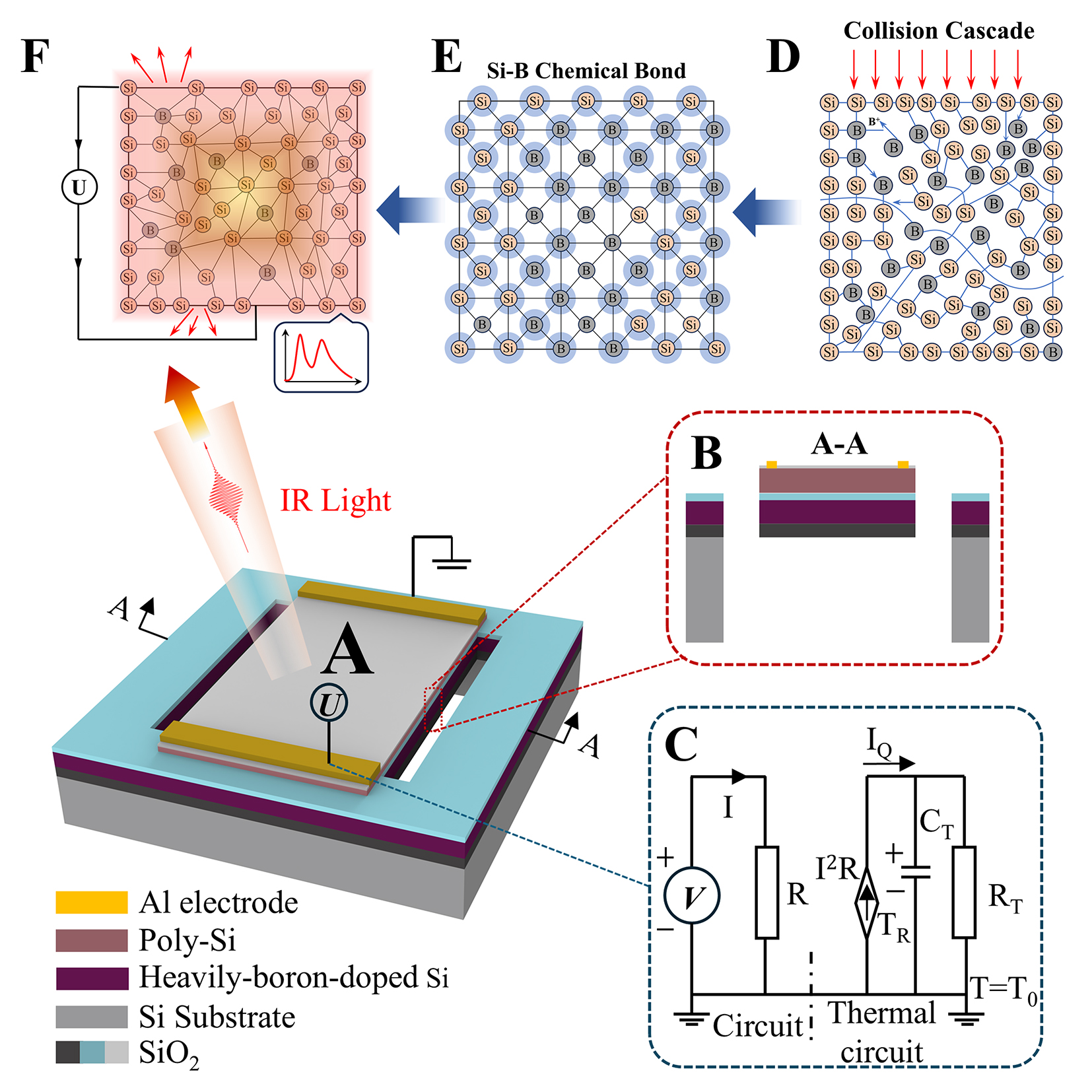
Figure 1. Schematic of the proposed MEMS infrared-light-source chip. (A) 3D model; (B) Cross-sectional view along the A-A plane; (C) Equivalent circuit diagram illustrating the working principle of the MEMS-based suspended membrane infrared-light-source chip; (D) Atomic distribution map of boron ion implantation; (E) Schematic of Si-B bond formation after annealing; (F) Atomic-level schematic of electrothermal radiation in B-doped polycrystalline silicon.
The operational principle of the MEMS infrared light source chip relies on Joule heating, which is analogous to a voltage-driven resistive self-heating circuit model[25], as shown in Figure 1C. In the thermal circuit, the ground symbol indicates that the reference temperature T0 is set to 0. CT and RT are the heat capacity of the emissive layer and its thermal resistance to the constant-temperature heat sink, respectively. In this model, the current variable includes the dimension of power, and the voltage across CT corresponds to the temperature increase ΔT of the emissive layer relative to T0 (the emissive layer temperature TR). The doped polysilicon thin film is equivalent to a resistor. Joule heat is generated under a constant voltage source, which increases the temperature and produces infrared radiation. At the molecular level, the bombardment of silicon lattices by high-energy boron ions triggers cascade collisions, displacing numerous silicon atoms from their lattice sites and forming high-density point defects, interstitials, and vacancies in the ordered crystal [Figure 1D]. Subsequent high-temperature annealing activates impurities, repairs lattice defects, and facilitates substitutional doping of boron atoms to form stable Si-B covalent bonds with silicon atoms
Numerical simulation
The structure of infrared-light-source chips must exhibit excellent radiative temperature and thermo-mechanical stability considering their performance and reliability requirements. Electrothermal-structural multiphysics coupling simulation analysis of these chips may be conducted with suspended, semi-closed, and closed membranes using a simulation platform[33,34]. The difference between these three structures lies in the extent of the backside substrate etching: complete etching was used for the suspended membrane, partial etching for the semi-closed membrane, and no etching for the closed membrane. The detailed simulation procedure is provided in Supplementary Tables 1 and 2. The radiation temperature of the infrared-light-source chip increases with the applied bias voltage
Simulation analysis was conducted to characterize the radiation temperature and thermal deformation behavior of different structures. As shown in Figure 2A, the radiation temperature of the suspended membrane infrared source chip is highly localized within the polysilicon film, exhibiting a pronounced thermal gradient that increases toward the central region. By contrast, Figure 2B and C shows that the radiation temperature in the semi-closed and closed membranes is more uniformly distributed across the device surface, exhibiting consistent overall thermal profiles. In terms of deformation, Figure 2D indicates that the deformation of the suspended membrane is mainly confined to the film region. By contrast,
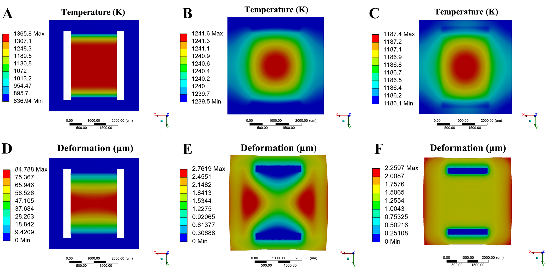
Figure 2. 3D electrothermal-structural multiphysics simulations of infrared-light-source chips. (A-C) Thermal distribution and deflection of the suspended, semi-closed, and closed membranes; (D-F) Deformation distribution and deflection of the suspended, semi-closed, and closed membranes.
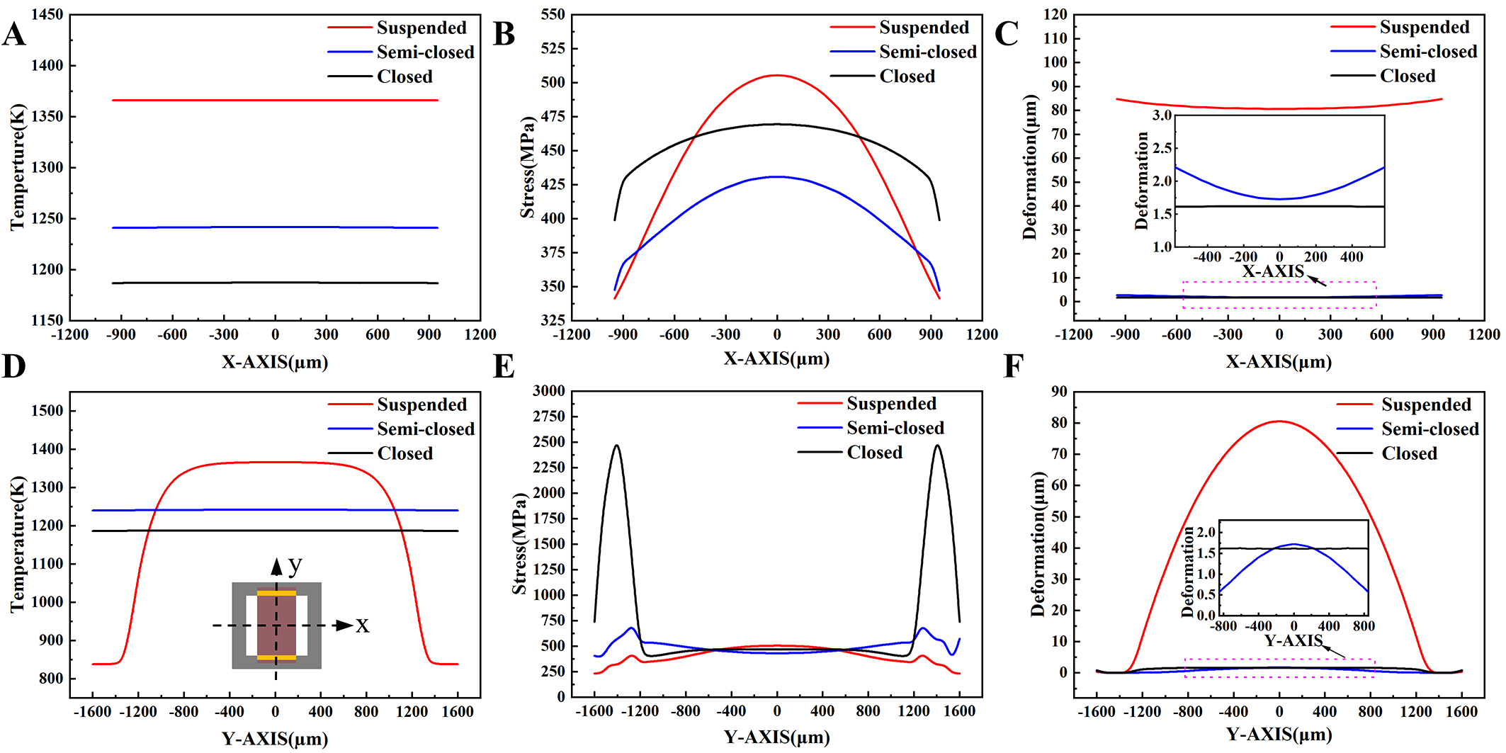
Figure 3. Curves of infrared-light-source chip temperature, stress, and deformation versus the center distance under a working voltage of 12 V. (A-C) Quantitative temperature, stress, and deformation data along the X-axis for suspended, semi-closed, and closed membrane infrared chips; (D-F) Quantitative temperature, stress, and deformation data along the Y-axis for the suspended, semi-closed, and closed membrane infrared chips.
As shown in Figure 3C and F, the suspended membrane displays V-shaped thermal deformation with marked central deflection. This occurs because radiant heat is highly concentrated in the central area of the membrane, and the absence of an underlying substrate support allows the film to buckle under thermal stress. By contrast, both the semi-closed and closed membranes, which have a more uniform temperature distribution, undergo a smaller balloon-like thermal deformation[35] across the entire structure. Based on the simulation results above, the suspended membrane structure, achieves a highly concentrated radiative temperature (up to 1,360 K at the center) owing to its thermal isolation characteristics while effectively reducing thermal stress accumulation through structural flexibility. This leads to a superior overall performance in both radiative output and thermomechanical reliability.
Nano characteristics
To verify the fabrication dimensions, step-height profilometry was performed on the front side of the 4-inch wafer [Figure 4A]. The measurement profile shows three distinct features: the evaporated aluminum electrode with a thickness of 1.35 µm, the combined polysilicon and overlying SiO2 layer with an etched depth of 0.79 µm (7,856 Å), and the deep-etched windows flanking the polysilicon structure, measured at 4.90 µm (48,950 Å). The internal material structure was further characterized using focused ion beam (FIB) milling. Figure 4B presents a cross-sectional FIB-scanning electron microscopy (SEM) image obtained perpendicular to the device surface, clearly delineating the interface between the Al electrode and polysilicon film. Corresponding energy-dispersive X-ray spectroscopy (EDS) elemental maps [Figure 4C-E] confirm the material composition within this region. The analysis reveals that aluminum is concentrated in the top electrode layer [Figure 4C], while oxygen is effectively confined to the intermediate thermally insulating SiO2 layer [Figure 4D]. Silicon is distributed throughout both the polysilicon film and underlying single-crystal substrate [Figure 4E]. Notably, boron dopants are not detected, and this is attributed to boron being an ultralight element. Its weak interaction with electrons results in characteristic X-rays of extremely low intensity, which are challenging to resolve via EDS[36,37]. Finally, Figure 4F-H respectively depicts the surface morphology of the fabricated polysilicon, overall chip layout, and final infrared light source in a TO-39 package showing both capped and open wire-bonded configurations.
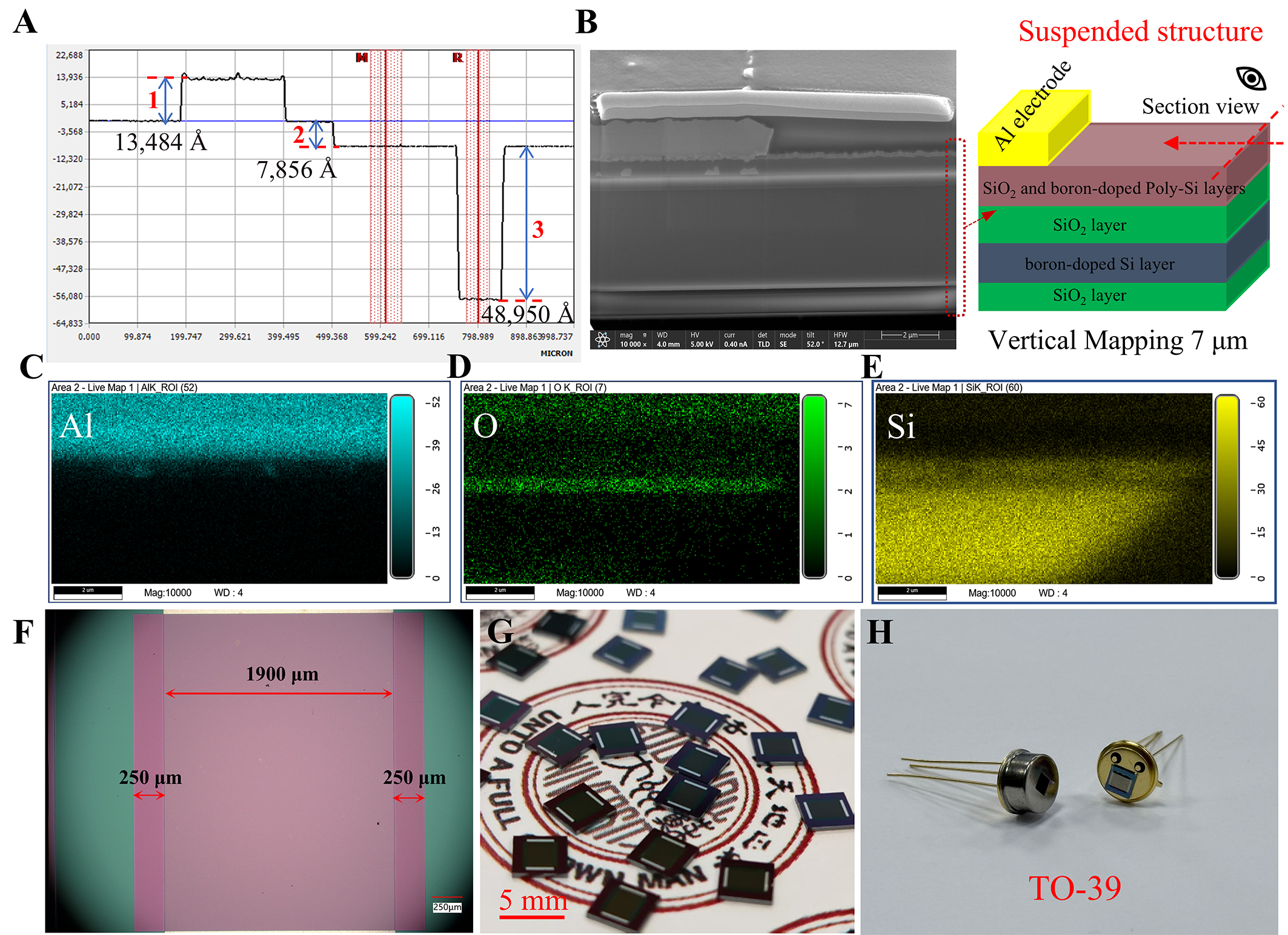
Figure 4. Structural characteristics of the MEMS infrared-light-source chip. (A) Step depth on the wafer surface; (B) FIB-SEM image of the suspended-membrane infrared-light-source chip; (C-E) EDS elemental distribution maps of Al, O, and Si; (F) Surface morphology of the fabricated polysilicon system; (G) Architecture of the infrared-light-source chip; (H) Infrared light source packaged in TO-39.
Temperature resistance coefficient
The current-voltage (I-V) profiles presented in Figure 5A and B reveal the critical role of membrane topology on device performance. Both the suspended and semi-closed membranes initiate with an identical resistance of 58 Ω. However, as the voltage increases, the suspended membrane undergoes a more rapid resistance increase, leading to a suppressed current relative to the semi-closed counterpart. This nonlinearity is a manifestation of the self-heating effect governed by the positive temperature coefficient of resistance (TCR) of the polysilicon layer[38]. This relationship can be approximated by the following simple linear equation:
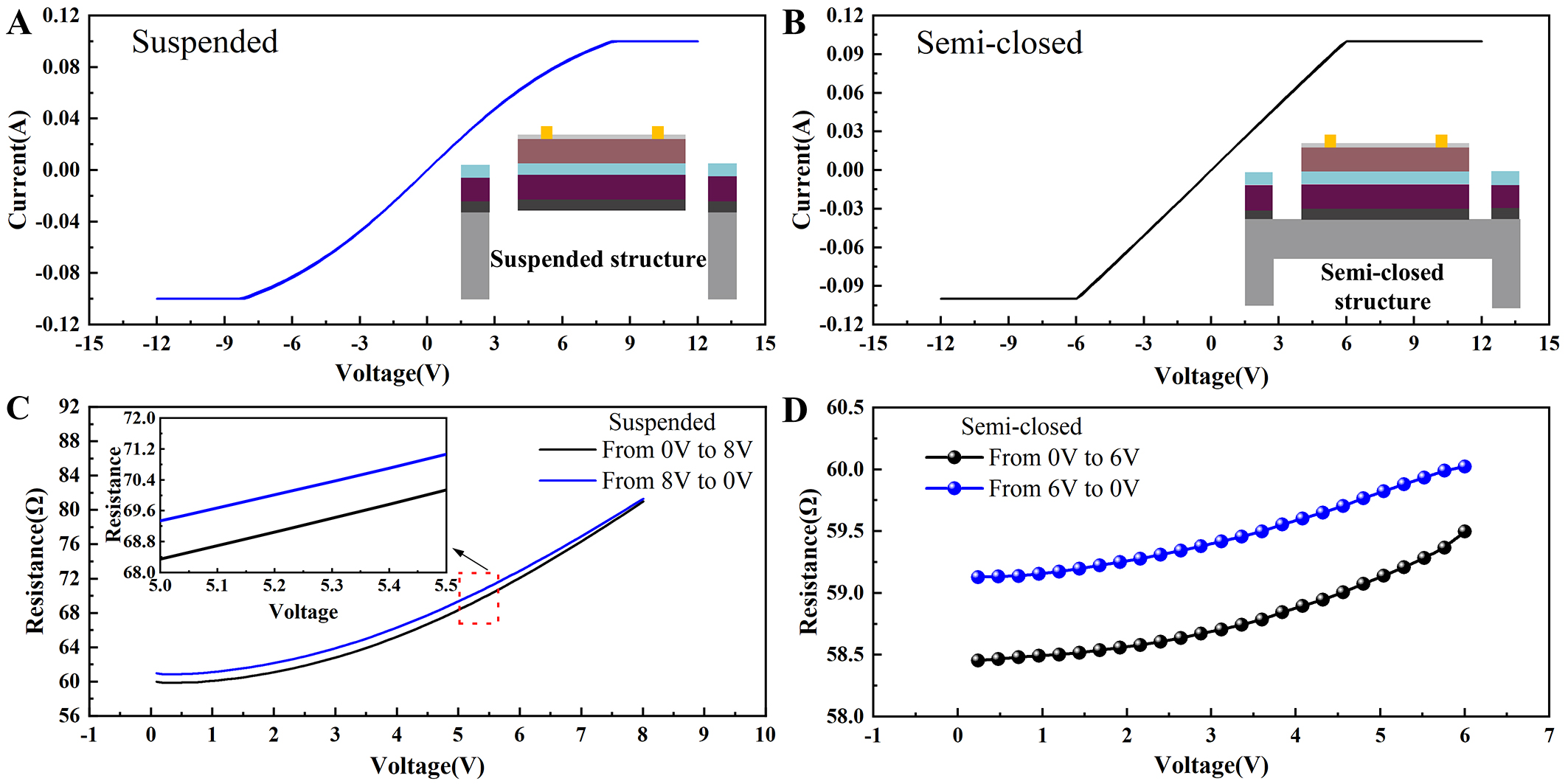
Figure 5. TCR of the suspended- and semi-closed-membrane infrared light sources. I-V curves of the (A) suspended and (B) semi-closed membranes; (C) Resistance range of the suspended membrane during forward and reverse voltage sweeps over 0-8 V; (D) Resistance range of semi-closed membrane during forward and reverse voltage sweeps over 0-6 V.
where αP represents the TCR of polysilicon and Rr is the resistance of polysilicon at room temperature Tr. Because polysilicon has a positive TCR[39], the resistance increases as the temperature increases. Crucially, the higher resistance (and consequently lower current) observed in the suspended membrane at a given voltage serves as direct evidence of its higher operating temperature. This confirms that the suspended architecture effectively suppresses backside thermal loss, resulting in superior heat localization compared to the semi-closed design (consistent with the simulation results in Figure 2A-C). Furthermore, the resistance-voltage (R-V) characteristics [Figure 5C and D] exhibit a hysteresis loop indicative of thermal inertia. During the reverse sweep, the release of stored thermal energy from the heavily boron-doped diffusion layer retards the cooling of the polysilicon, causing a transient resistance elevation. Despite this thermal lag, the suspended source exhibits excellent electrothermal stability with a wide operational window[40].
Electrothermal characteristics
Supplementary Figure 11 shows the experimental platform used for the electrothermal characterization of the infrared light source. As shown in Figure 6A, the infrared radiation temperature of both membranes increased approximately linearly with the staircase voltage from 5 to 12 V (step size: 0.5 V). However, substantial temperature differences were observed for the suspended (726.15 K) and semi-closed (559.85 K) membranes. Under the same voltage conditions, the infrared radiation temperature of the suspended membrane was higher than that of the semi-closed membrane, and it exhibited a faster heating rate. To further explore the correlation between power consumption and temperature, a digital source meter was used to record the resistance and power consumption of the devices at 5 to 12 V. The power consumption-temperature curves of the suspended and semi-closed membrane infrared sources in Figure 6B were obtained by combining these experimental data with the voltage-temperature curve shown in
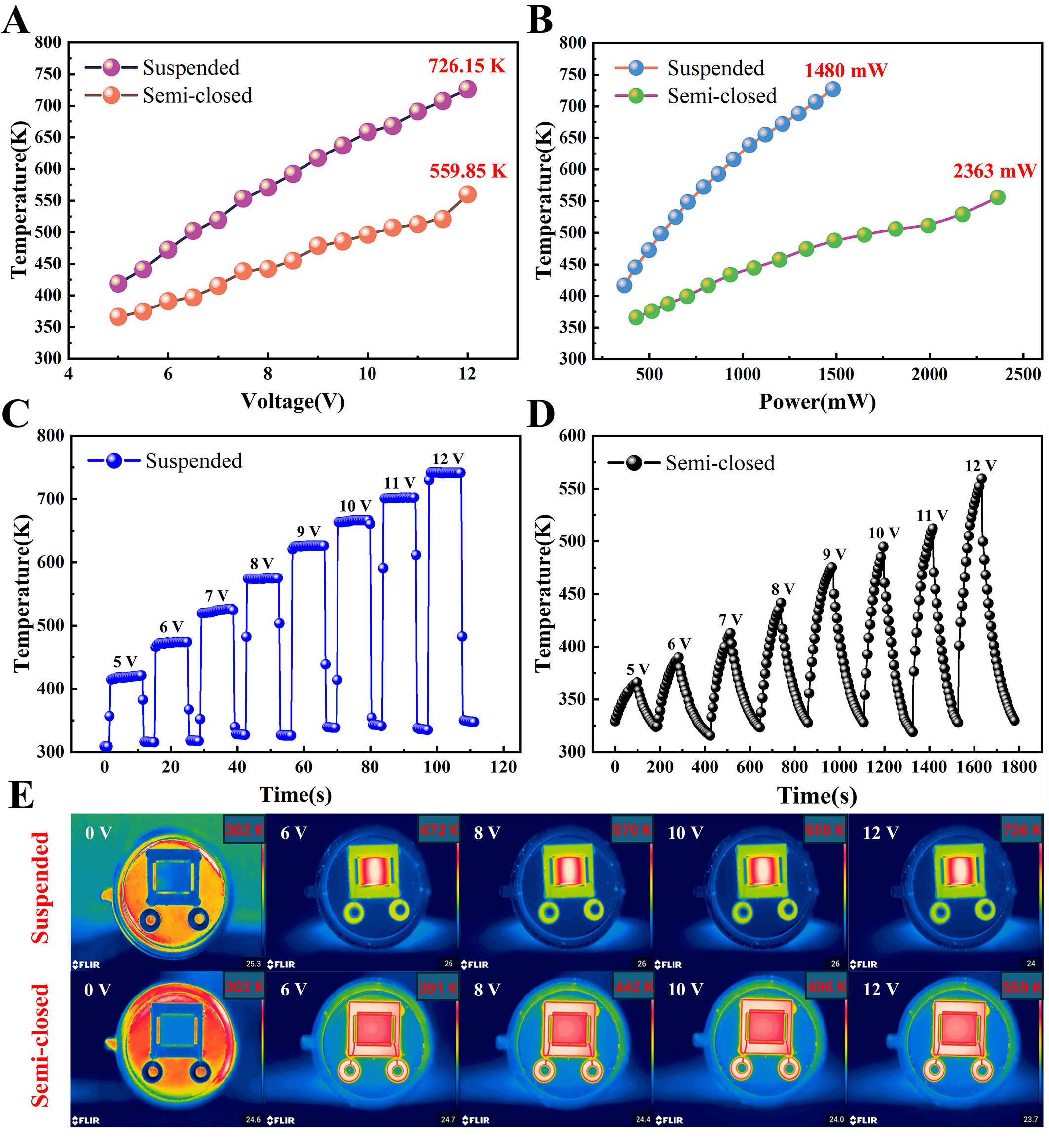
Figure 6. Electrothermal characteristics of the suspended- and semi-closed-membrane infrared light sources. (A) Voltage-radiation temperature curve of the infrared light source; (B) Power consumption-temperature curve of the infrared light source; Continuous electrothermal modulation curves of the (C) suspended and (D) semi-closed membranes; (E) Surface radiation temperature maps of the suspended and semi-closed membranes at different temperatures.
Next, the dynamic performances of the devices were investigated. The suspended and semi-closed membrane infrared sources were driven by a signal generator that produced a pulsed waveform with a 50% duty cycle at voltages of 5 to 12 V, and the temperature was measured using an IR thermal camera.
The thermal flux of the infrared light source, which represents the density and intensity of infrared energy flow, is a key metric used for electrothermal performance evaluation. Thermal flux comparisons of different structures [Figure 7A and B] show that the suspended membrane delivers the highest thermal flux, directly verifying that it exhibits the highest infrared radiation temperature among the evaluated systems. Thermal flux data for the semi-closed membrane is presented in Supplementary Figure 13. This excellent performance arises from the unique thermal management mechanism of the suspended membrane, wherein the back cavity and isolation trenches of the suspended membrane effectively block solid heat conduction to the silicon substrate. This confines heat mainly inside of the membrane for convective exchange with ambient air [Figure 7A]. This design greatly reduces the lateral heat loss of the substrate, effectively converting electrical energy into an increase in radiation temperature. In addition, this design improves the rapid thermal response of the device owing to the low thermal capacity and fast response of heat exchange with air.
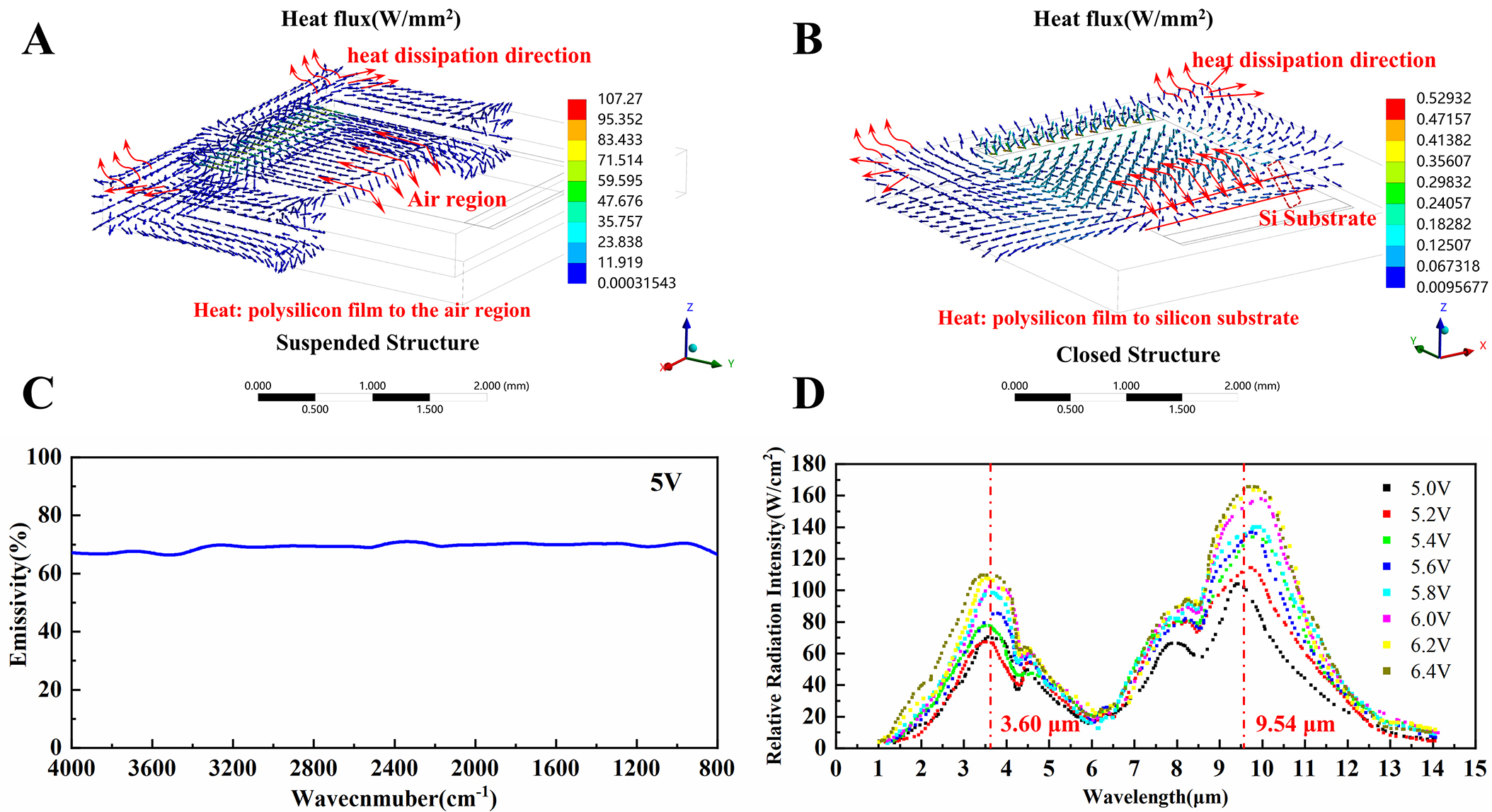
Figure 7. Thermal flux and IR radiation spectra of the infrared light source. Schematic of the thermal flux of the (A) suspended- and (B) closed-membrane infrared-light-source chips; (C) Infrared emissivity under an applied voltage of 5 V; (D) Infrared radiation intensity under continuous voltage variation from 5 to 6.4 V.
The spectral emissivity within the 2.5-12.5 μm range was characterized using an FTIR spectrometer coupled with an integrating sphere and microscope, as illustrated in Supplementary Figure 14. In accordance with Kirchhoff's law[43], the emissivity of the infrared source is given by:
where ε, α, ρ, and τ denote emissivity, absorptivity, reflectivity, and transmittance, respectively. Given the opacity of the SOI substrate in this band, the τ is zero; therefore, Equation (2) can be alternatively expressed as Equation (3), where emissivity is complementary to reflectivity. As shown in Figure 7C, the device maintains a high, stable emissivity of approximately 0.7 under a 5 V DC bias. This performance is structurally governed by the heavy boron doping of the polysilicon film. The high dopant concentration introduces a dense population of positively charged holes[44], which markedly enhances free-carrier absorption. This mechanism effectively suppresses infrared reflection and promotes photon absorption, thereby intrinsically elevating the thermal emissivity of the radiating layer.
The infrared radiation intensity was quantified using a full-band solar spectral radiometer
where c is the speed of light, λ is the wavelength, K is the Boltzmann constant, h is Planck’s constant, Ta is the absolute temperature of the radiating surface, and IB is the radiated power per unit area per unit solid angle per unit wavelength. Figure 7D details the spectral radiance with increasing DC bias from 5 to 6.4 V. The spectrum exhibits a dual-band profile shaped by the molecular vibrational modes of the material. In particular, a short-wave band (1.0-5.92 μm, centered at 3.60 μm) and long-wave band (5.92-14 μm, centered at 9.54 μm) are observed. At 6.4 V, the long-wave band dominates, contributing ~60% of the total energy with a peak intensity of 170 W/cm², compared to 110 W/cm² (~40%) for the short-wave band. With increasing driving voltage, the infrared radiation temperature and relative radiation intensity of all bands exhibit a corresponding increase. Crucially, these characteristic spectral peaks result from the synergistic effect of carrier plasmon resonance[46,47] and characteristic lattice vibrational modes[48,49] in heavily boron-doped poly-Si. The 3.6-μm characteristic peak arises from an enhancement in the narrowband resonant emissivity induced by the stretching vibrations of hydrogen-bond-bridged Si-O and oxygen-vacancy-associated Si-H bonds in the short-wave infrared plasmon enhancement window[50,51]. The intense 9.54 μm emission peak stems from the spectral superposition of the Si-O bending and Si-B stretching vibrations (introduced by boron implantation at a 7 × 1019 cm-3 doping concentration) in the long-wave infrared plasmon enhancement window[52-55]. This characteristic spectral signature verifies that the emission spectrum of the MEMS source matches the absorption bands of target gases in non-dispersive infrared sensing applications.
Modulation depth
The modulation dynamics of the infrared source were characterized via pulsed electrical heating and subsequent self-cooling[38]. The experimental setup for the modulation performance characterization of the infrared light source is shown in Supplementary Figure 16. The optical response was recorded using a spectroradiometer with a 50% duty cycle driving signal [Figure 8A]. Figure 8B shows the time-domain response at 1, 5, and 50 Hz, where a characteristic attenuation in peak voltage was observed with increasing frequency. The transient response was quantified using the rise time (tr, 0%-90% of the peak value) and fall time (tf, 100%-10% of the peak value)[56]. At 5 Hz, the device exhibited a tr of 36 ms and tf of 28 ms, yielding a total switching period of 64 ms [Figure 8C]. This rapid response is structurally enabled by the suspended membrane design. While the backside cavity provides high thermal resistance to isolate the membrane from the substrate, thereby minimizing power consumption, the extremely low thermal mass of the thin membrane ensures that thermal inertia remains low. This unique structural combination enables rapid thermal cycling despite high thermal isolation, thereby simultaneously reducing power consumption. The modulation depth of an infrared source is defined as the maximum voltage variation at a given modulation frequency, normalized to the reference voltage variation at the baseline frequency. The modulation depth (m) is then determined from the peak response voltage using[57]:
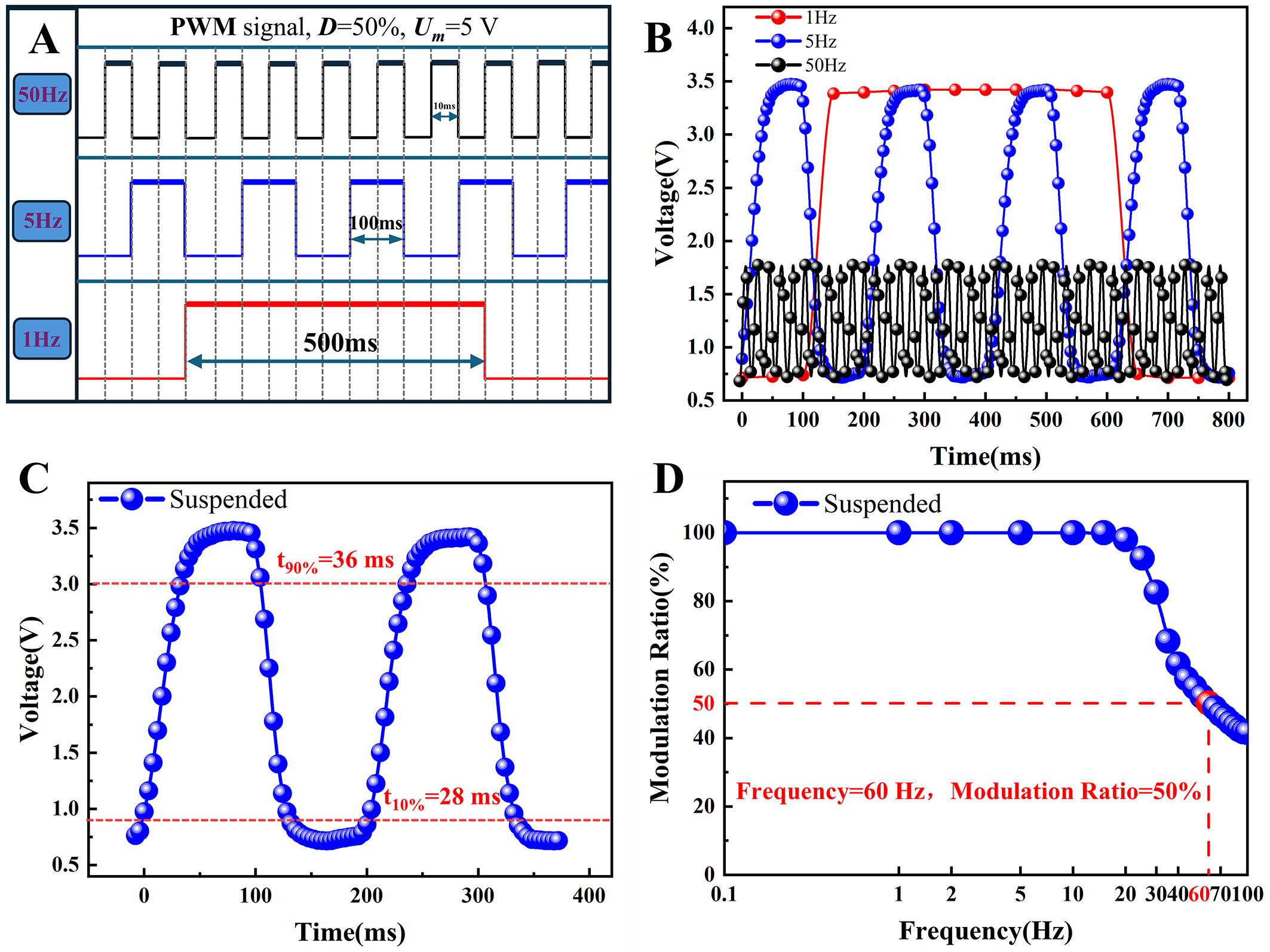
Figure 8. Modulation performance of the suspended membrane infrared source. (A) Schematic of a square wave with 50% pulse width modulation duty cycle generated by a signal generator; (B) Time-domain response of the infrared source at 1, 5, and 50 Hz; (C) Switching time of the infrared source; (D) Modulation depth of the infrared source.
Herein, the modulation depth at 1 Hz was defined as 100%, where Vmax(f) and Vmin(f) represent the maximum and minimum voltage values at the current frequency f, respectively, and Vmax(1Hz) and Vmin(1Hz) represent the maximum and minimum voltage values at 1 Hz, respectively. Figure 8D presents the measured modulation depth curve of the suspended-membrane infrared light source. A 100% modulation depth was maintained for operating frequencies up to 15 Hz, after which a gradual decrease was observed, exhibiting a roll-off of 41% at a frequency of 100 Hz. At 20 Hz, the modulation depth remained at 98%, indicating that highly stable infrared radiation could be emitted under pulsed driving conditions. At 50 Hz, approximately 55% of the infrared energy was measured. These findings indicate the exceptional efficiency of the suspended-membrane infrared light source when operated with pulsed driving.
The electrical-to-optical conversion efficiency is a critical metric for evaluating the radiative efficiency of infrared light sources[58], which directly reflects the technological advancement of the light source in terms of material quality, carrier injection efficiency, and photon extraction efficiency. The detailed experimental platform is shown in Supplementary Figure 17, and the corresponding methodological details are provided in the Supplementary Materials. The suspended membrane infrared light source achieved an electro-optical conversion efficiency of 12.33% at a driving voltage of 7 V [Supplementary Table 3], which indicates that heavy boron-ion doping in polycrystalline silicon resulted in an enhanced carrier injection efficiency. Moreover, the photon extraction efficiency was indirectly improved via the regulation of the doping concentration, processing parameters, and lattice defects, which served to improve the infrared radiation performance. Table 1 presents a comparison of the MEMS infrared emitter developed in this study with those reported in the literature to evaluate the comprehensive performance of the suspended-membrane infrared light source. The fabricated device features a large radiating area, desirable modulation depth, dual-band central emission, and highly stable radiation temperature. In addition, it achieved a higher modulation depth and faster response time compared with bulk infrared emitters based on MPE, c-Si, and Pt. Moreover, it delivers dual-wavelength radiation, which is absent in conventional TiN and Pt-black infrared emitters.
Performance comparison with of previously developed MEMS IR emitters
| Modulation depth-frequency (Hz) | Response time (ms) | Central band (μm) | Emissivity | Temperature (°C) | Radiation area (mm2) | Heater material | References |
| 65.6%-100% | 31 | 3.8 | 0.6 | 408 | 0.062 | TiN | [38] |
| 42%-100% | 17 | N/A | 0.99 | 407 | 1 | Pt-black | [59] |
| N/A | N/A | 3.96 | 0.99 | 322 | 2.89 | MPE | [20] |
| 50%-20% | 53.8 | N/A | N/A | 800 | 0.33 | c-Si | [60] |
| 50%-40% | 58 | 6.5 | N/A | 450 | 2.25 | Pt | [61] |
| 50%-60% | 36 | 3.6 and 9.54 | 0.7 | 450 | 6.08 | poly-Si | This work |
CONCLUSIONS
In this study, a high-performance MEMS infrared radiation source with an optimized suspended architecture was developed to address the modulation depth and spectral emission range limitations of conventional thermal infrared emitters. An ultrathin suspended-membrane infrared-light-source based on a silicon-on-insulator wafer was designed and fabricated. This design enabled the targeted optimization of the thermal isolation performance and thermal mass of the device, whose parameters significantly affect the modulation speed and energy efficiency of thermal emitters. The fabricated device exhibited exceptional electrothermal characteristics and unique spectral properties, providing a robust and promising platform for infrared applications requiring high-efficiency, high-speed modulation. Furthermore, the developed device exhibited excellent compatibility with standard CMOS processes. Therefore, this work outlines a cost-effective, highly scalable method for developing next-generation optical recognition systems and high-sensitivity gas-sensing devices.
DECLARATIONS
Authors’ contributions
Design: Zhu, K.; Li, R.; He, J.
Experiments: Zhu, K.; Zhang, Y.
Original draft, investigation, data curation: Li, R.; Lan, Z.; Wang, Y.
Manuscript writing: Zhu, K.; Li, R.;
Language revision: Zhu, K.; Zhai, J.
Manuscript revision and supervision: Wang, J.; Chen, T.; Chou, X.; He, J.
Availability of data and materials
The raw data supporting the findings of this study are available within this Article and its Supplementary Materials. Further data are available from the corresponding authors upon request.
AI and AI-assisted tools statement
Not applicable.
Financial support and sponsorship
The authors gratefully acknowledge financial support from the National Natural Science Foundation of China (Grants No. U23A20639, 52375571 and 62573309), the China Postdoctoral Science Foundation (No. 2024M764266), and the Suzhou Frontier Technology Research Projects (No. SYG202322).
Conflicts of interest
All authors declared that there are no conflicts of interest.
Ethical approval and consent to participate
Not applicable.
Consent for publication
Not applicable.
Copyright
© The Author(s) 2026.
Supplementary Materials
REFERENCES
1. Shi, W.; Guo, R.; Tian, G.; et al. A broadband self-powered and stable photothermoelectric detector based on Ag2Se/MWCNTs composite fabricated via screen printing. Microstructures 2025, 5, 2025081.
2. Zhao, X.; Dai, J.; Li, L.; Su, Z.; Ma, X. Deep learning-based laser and infrared composite imaging for armor target identification and segmentation in complex battlefield environments. Infrared. Phys. Technol. 2023, 132, 104725.
3. Zha, J.; Shi, S.; Chaturvedi, A.; et al. Electronic/optoelectronic memory device enabled by tellurium‐based 2D van der Waals heterostructure for in‐sensor reservoir computing at the optical communication band. Adv. Mater. 2023, 35, 2211598.
4. Xiong, J.; Yu, Q.; Hou, X.; et al. Short‐wave infrared photodetectors based on β‐In2Se3/Te heterojunctions for optical communication and polarimetric imaging applications. Adv. Funct. Mater. 2024, 34, 2314972.
5. Zhang, Y.; Yin, P.; Song, F.; et al. A chemiresistive MEMS acetone gas sensor based on p-Rh2O3-n-WO3 heterostructure for diagnosing diabetes and monitoring diabetic states. Sens. Actuators. B. Chem. 2025, 442, 138110.
6. Feng, L.; Liu, Y.; Wang, Y.; Zhou, H.; Wu, M.; Li, T. An ultra-small integrated CO2 infrared gas sensor for wearable end-tidal CO2 monitoring. iScience 2023, 26, 108293.
7. Yun, J.; Ahn, J.; Moon, D.; Choi, Y.; Park, I. Joule-heated and suspended silicon nanowire based sensor for low-power and stable hydrogen detection. ACS. Appl. Mater. Interfaces. 2019, 11, 42349-57.
8. Saha, P.; Mukhopadhyay, S. Multispectral information fusion with reinforcement learning for object tracking in IoT edge devices. IEEE. Sensors. J. 2020, 20, 4333-44.
9. Kinjalk, K.; Paciolla, F.; Sun, B.; et al. Highly selective and sensitive detection of volatile organic compounds using long wavelength InAs-based quantum cascade lasers through quartz-enhanced photoacoustic spectroscopy. Appl. Phys. Rev. 2024, 11, 021427.
10. Stark, D.; Kapsalidis, F.; Markmann, S.; et al. Quantum cascade surface emitting lasers. Laser. Photonics. Rev. 2024, 18, 2300663.
11. Wu, D.; Mo, Z.; Li, X.; et al. Integrated mid-infrared sensing and ultrashort lasers based on wafer-level Td-WTe2 Weyl semimetal. Appl. Phys. Rev. 2024, 11, 041401.
12. Gao, L.; Quan, L. N.; García De Arquer, F. P.; et al. Efficient near-infrared light-emitting diodes based on quantum dots in layered perovskite. Nat. Photonics. 2020, 14, 227-33.
13. Li, G.; Chen, X.; Wang, M.; et al. Multiband excited bright NIR emitter via Yb3+/Cr3+ co-doped double perovskites for multimodal anti-counterfeiting and imaging. J. Lumin. 2025, 287, 121488.
14. Deng, X.; Chen, X.; Wang, M.; et al. Multicolor and multimode luminescent lanthanide-doped Cs2NaInCl6:Sb3+ from visible to near infrared for versatile applications. J. Lumin. 2025, 277, 120908.
15. Wu, X.; Li, J.; Xie, F.; et al. A dual-selective thermal emitter with enhanced subambient radiative cooling performance. Nat. Commun. 2024, 15, 815.
16. Du, K.; Li, Q.; Lyu, Y.; et al. Control over emissivity of zero-static-power thermal emitters based on phase-changing material GST. Light. Sci. Appl. 2016, 6, e16194-.
17. Li, D.; Liu, X.; Li, W.; et al. Scalable and hierarchically designed polymer film as a selective thermal emitter for high-performance all-day radiative cooling. Nat. Nanotechnol. 2020, 16, 153-8.
18. Razeghi, M.; Lu, Q. Y.; Bandyopadhyay, N.; et al. Quantum cascade lasers: from tool to product. Opt. Express. 2015, 23, 8462.
19. Veldhuis, S. A.; Boix, P. P.; Yantara, N.; et al. Perovskite materials for light‐emitting diodes and lasers. Adv. Mater. 2016, 28, 6804-34.
20. Lochbaum, A.; Fedoryshyn, Y.; Dorodnyy, A.; Koch, U.; Hafner, C.; Leuthold, J. On-chip narrowband thermal emitter for mid-IR optical gas sensing. ACS. Photonics. 2017, 4, 1371-80.
21. Li, K.; Liang, Y.; Lin, Y. MEMS-based meta-emitter with actively tunable radiation power characteristic. Discover. Nano. 2024, 19, 133.
23. Mele, L.; Santagata, F.; Iervolino, E.; et al. A molybdenum MEMS microhotplate for high-temperature operation. Sens. Actuators. A. Phys. 2012, 188, 173-80.
24. Lee, K.; Lee, D.; Jung, S.; Jang, Y.; Kim, Y.; Seong, W. A high-temperature MEMS heater using suspended silicon structures. J. Micromech. Microeng. 2009, 19, 115011.
25. Lai, L.; Liu, P.; Zhou, D.; Li, Q.; Fan, S.; Lu, W. Rapidly modulated wide‐spectrum infrared source made of super aligned carbon nanotube film for greenhouse gas monitoring. Adv. Funct. Mater. 2022, 33, 2208891.
26. Wu, Z.; Wu, Z.; Lv, H.; et al. Nanophotonic catalytic combustion enlightens mid-infrared light source. Nano. Res. 2023, 16, 11564-70.
27. Chang, W.; Hsihe, Y. Multilayer microheater based on glass substrate using MEMS technology. Microelectron. Eng. 2016, 149, 25-30.
28. Ng, D. K. T.; Ho, C. P.; Xu, L.; et al. NDIR CO2 gas sensing using CMOS compatible MEMS ScAlN-based pyroelectric detector. Sens. Actuators. B. Chem. 2021, 346, 130437.
29. Wei, W.; He, A.; Yang, B.; et al. Monolithic integration of embedded III-V lasers on SOI. Light. Sci. Appl. 2023, 12, 84.
30. Wei, Y.; Liu, G.; Wei, J.; et al. Revealing the structure of SiO2 and its effects on electrical properties. Mater. Today. Commun. 2024, 38, 107874.
31. Liu, H.; Zhao, M.; Gong, Y.; et al. A high precision and multifunctional electro-optical conversion efficiency measurement system for metamaterial-based thermal emitters. Sensors 2022, 22, 1313.
32. Sahel, S.; Amri, R.; Bouaziz, L.; et al. Optical filters using Cantor quasi-periodic one dimensional photonic crystal based on Si/SiO2. Superlattices. Microstruct. 2016, 97, 429-38.
33. Hassan, S.; Rajaguru, P.; Stoyanov, S.; Bailey, C.; Tilford, T. Coupled thermal-mechanical analysis of power electronic modules with finite element method and parametric model order reduction. Power. Electron. Devices. Compon. 2024, 8, 100063.
34. Loche-moinet, F.; Theolier, L.; Woirgard, E. Electro-thermo-mechanical modelling of a SiC MOSFET transistor under non-destructive short-circuit. Microelectron. Reliab. 2023, 150, 115143.
35. Nejat Pishkenari, H.; Mohagheghian, E.; Rasouli, A. Molecular dynamics study of the thermal expansion coefficient of silicon. Phys. Lett. A. 2016, 380, 4039-43.
36. Wang, M.; You, S.; Cheng, Y.; et al. Difference of carrier dynamics in a semiconductor saturable absorber mirror with and without B+ ion-implantation. Appl. Opt. 2024, 63, 1947.
37. Aitkaliyeva, A.; Mccarthy, M. C.; Jeong, H.; Shao, L. Irradiation studies on carbon nanotube-reinforced boron carbide. Nucl. Instrum. Methods. Phys. Res. B. 2012, 272, 249-52.
38. Ding, P.; Su, Y.; Huang, J.; et al. Design, fabrication, and characterization of a low-power, high-modulation-depth infrared emitter array. Int. J. Optomechatronics. 2025, 19, 2563509.
39. Chuang, H. M.; Thei, K. B.; Tsai, S. F.; Liu, W. C. Temperature-dependent characteristics of polysilicon and diffused resistors. IEEE. Trans. Electron. Devices. 2003, 50, 1413-5.
40. Beckel, D.; Briand, D.; Bieberle-Hütter, A.; Courbat, J.; De Rooij, N. F.; Gauckler, L. J. Micro-hotplates—A platform for micro-solid oxide fuel cells. J. Power. Sources. 2007, 166, 143-8.
41. Li, S.; Zhai, Y.; Dong, Y.; Cai, J.; Wang, M. Suspended insulation structure design for infrared thermal detector. J. Microelectromech. Syst. 2025, 34, 92-9.
42. Lefebvre, A.; Costantini, D.; Brucoli, G.; Boutami, S.; Greffet, J.; Benisty, H. Influence of emissivity tailoring on radiative membranes thermal behavior for gas sensing applications. Sens. Actuators. B. Chem. 2015, 213, 53-8.
43. Ali, S. Z.; De Luca, A.; Hopper, R.; Boual, S.; Gardner, J.; Udrea, F. A low-power, low-cost infra-red emitter in CMOS technology. IEEE. Sensors. J. 2015, 15, 6775-82.
44. Li, Y.; Yang, Y.; Chou, T.; et al. Carrier activation at end-of-range (EOR) defects and grain boundaries in boron-doped silicon. J. Electron. Mater. 2025, 54, 2211-8.
45. Choudhury, S. L.; Paul, R. A new approach to the generalization of Planck’s law of black-body radiation. Ann. Phys. 2018, 395, 317-25.
46. Zhang, H.; Zhang, R.; Schramke, K. S.; et al. Doped silicon nanocrystal plasmonics. ACS. Photonics. 2017, 4, 963-70.
47. Faruque, M. O.; Al Mahmud, R.; Sagor, R. H. Heavily doped silicon: a potential replacement of conventional plasmonic metals. J. Semicond. 2021, 42, 062302.
48. Würfl, J.; Palacios, T.; Xing, H. G.; Hao, Y.; Schubert, M. Special topic on Wide- and ultrawide-bandgap electronic semiconductor devices. Appl. Phys. Lett. 2024, 125, 070401.
49. Zhu, Y.; Li, Y.; Ding, H.; et al. Vibrational and structural insight into silicate minerals by mid-infrared absorption and emission spectroscopies. Phys. Chem. Miner. 2022, 49, 6.
50. Lin, S. Vibrational local modes of a-SiO2:H and variation of local modes in different local environments. J. Appl. Phys. 1997, 82, 5976-82.
51. Li, P.; Jiang, Y.; Hu, Y.; et al. Hydrogen bond network connectivity in the electric double layer dominates the kinetic pH effect in hydrogen electrocatalysis on Pt. Nat. Catal. 2022, 5, 900-11.
52. Privitera, V.; Napolitani, E.; Priolo, F.; et al. Atomic transport properties and electrical activation of ultra-low energy implanted boron in crystalline silicon. Mater. Sci. Semicond. Process. 1999, 2, 35-44.
53. Mcpolin, C. P. T.; Romero-Gómez, M.; Krasavin, A. V.; Dickson, W.; Zayats, A. V. Reconfigurable cavity-based plasmonic platform for resonantly enhanced sub-bandgap photodetection. J. Appl. Phys. 2020, 128, 203101.
54. Aziza, S.; Ripp, A.; Horvitz, D.; Rosenwaks, Y. Control of polysilicon nanowires conductivity by angle-dependent ion implantation. Mater. Sci. Semicond. Process. 2018, 75, 43-50.
55. Du, H.; Zhang, X.; Liu, W.; et al. High-performance boron emitters for tunnel oxide passivating contact solar cells enabled by multi-layer PECVD-deposited boron source structures. Chem. Eng. J. 2025, 515, 163487.
56. Vasilopoulou, M.; Fakharuddin, A.; García De Arquer, F. P.; et al. Advances in solution-processed near-infrared light-emitting diodes. Nat. Photonics. 2021, 15, 656-69.
57. Liu, W.; Ming, A.; Ren, Y.; et al. CMOS MEMS infrared source based on black silicon. In 2016 IEEE 11th Annual International Conference on Nano/Micro Engineered and Molecular Systems (NEMS); 2016 Apr 17-20; Sendai, Japan. IEEE; 2016. pp. 200-4.
58. Zhao, B.; Assawaworrarit, S.; Santhanam, P.; Orenstein, M.; Fan, S. High-performance photonic transformers for DC voltage conversion. Nat. Commun. 2021, 12, 4684.
59. Shu, D.; Tao, J.; Li, Y.; Fan, X. A miniature infrared emitter with ultra-high emissivity. In 2021 IEEE 16th International Conference on Nano/Micro Engineered and Molecular Systems (NEMS); 2021 Apr 25-29; Xiamen, China. IEEE; 2021. pp. 1175-8.
60. Calaza, C.; Salleras, M.; Sabaté, N.; Santander, J.; Cané, C.; Fonseca, L. A MEMS-based thermal infrared emitter for an integrated NDIR spectrometer. Microsyst. Technol. 2012, 18, 1147-54.
Cite This Article
How to Cite
Download Citation
Export Citation File:
Type of Import
Tips on Downloading Citation
Citation Manager File Format
Type of Import
Direct Import: When the Direct Import option is selected (the default state), a dialogue box will give you the option to Save or Open the downloaded citation data. Choosing Open will either launch your citation manager or give you a choice of applications with which to use the metadata. The Save option saves the file locally for later use.
Indirect Import: When the Indirect Import option is selected, the metadata is displayed and may be copied and pasted as needed.
About This Article
Copyright

Data & Comments
Data
0


Comments
Comments must be written in English. Spam, offensive content, impersonation, and private information will not be permitted. If any comment is reported and identified as inappropriate content by OAE staff, the comment will be removed without notice. If you have any queries or need any help, please contact us at [email protected].