


Microstructure and piezoelectric properties of AC poled relaxor-PbTiO3 perovskite single crystals

 ,
, Abstract
High-performance perovskite relaxor-PbTiO3 (relaxor-PT) piezoelectric single crystals (SCs) fabricated by the melt-growth Bridgeman method have been widely used in medical ultrasound imaging devices as probes and in high-performance underwater equipment since around 2,000. To improve the piezoelectric properties of these SCs, the use of alternating-current poling (ACP) instead of conventional DC poling has been widely adopted since 2018. Macro- and microstructural observations by scanning electron microscopy (SEM) are the best way to easily confirm the relationship between electrical properties and macro- and microstructure. After optimal ACP, fine 109° domain layers of 0.5 to several µm parallel to the electrodes have been obtained, contributing to 10%-100% improvement in dielectric constant and piezoelectric constant. Relaxor-PT SCs fabricated by the solid state crystal growth method with self-poring, excellent composition uniformity and machinability, high piezoelectric performance, and the low acoustic impedance due to the inclusion of spherical micropores in the SCs are also discussed.

Keywords
INTRODUCTION
Piezoelectric materials possess a distinctive capacity to transform mechanical energy into electrical energy and vice versa. Piezoelectric materials take many forms, including crystals, ceramics, and inorganic or organic thin films. Until now, PZT ceramics have been the representative piezoelectric material, but since 2000, relaxor single crystals with higher performance have been widely used in advanced fields[1-5]. These piezoelectric materials are utilized in a multitude of applications, including medical ultrasound diagnostic equipment, marine sonar, actuators, acceleration sensors, filters and ultrasonic processing machines. They contribute to social development and have become indispensable elements for various industrial and academic applications. For instance, the global market for ultrasound diagnostic equipment is projected to reach US $ 8.5 billion in 2023, with an anticipated annual growth rate of 5.3% from 2024 to 2028, culminating in a valuation of US $ 12.5 billion in 2028, as illustrated in Figure 1A. Relaxor-PT single crystal (SC) ingot-based ultrasonic transducers, exemplified by those depicted in Figure 1B, as well as transducers illustrated in Figure 1C and D, have been produced and utilized in over a million units over the past two decades. It is estimated that SC-based ultrasonic transducers currently represent over 30% of the total transducer market in terms of sales.
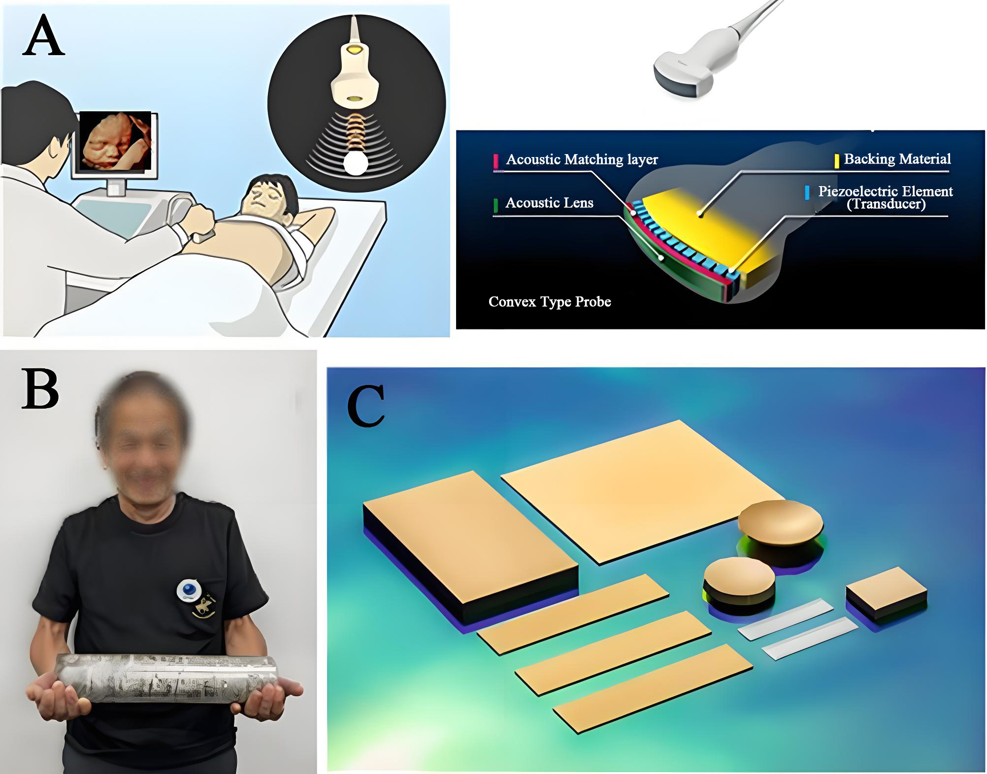
Figure 1. (A) Echo ultrasound imaging equipment; (B) medical array probe; (C) PMN-PT Single crystal ingot (D80 × L320 mm, 13 kg, courtesy of JFE Mineral Co. Japan); and (D) medical single crystal transducers. PMN: Pb(Mg1/3Nb2/3)O3; PT: PbTiO3.
Up until this point, Pb(Zr,Ti)O3 (PZT) ceramics or relaxor Pb(Me, Nb)O3 (Me = Mg, Zn, and In, etc.) - PbTiO3 (PT) piezoelectric single crystals have been polarized in a direct current (DC) electric field Direct Current Poling (DCP) in order to obtain their piezoelectric properties and subsequently apply them[3-5]. In 2014, Yamamoto and Yamashita et al. reported on the development of Pb(Mg1/3Nb2/3)O3 (PMN)-PT-based binary SCs and Pb(In1/2Nb1/2)O3 (PIN)-PMN-PT-based ternary SCs. The application of an alternating current (AC) electric field to PIN-PMN-PT-based ternary SCs results in the attainment of superior dielectric and piezoelectric characteristics through a process known as alternating current polarization (ACP)[6,7]. In light of these findings, numerous ACP-related studies have been conducted globally in recent years[8-71]. It is established that the dielectric and piezoelectric properties of ferroelectric piezoelectric materials are closely associated with the domain structure of ferroelectrics. A ferroelectric domain is a region inside a ferroelectric material where the polarization directions are aligned. Usually, ferroelectric domains with different polarization directions are mixed inside a ferroelectric material. The boundary surface where the domains meet is called a ferroelectric domain wall. When an external electric field is applied, the polarization of the entire crystal changes as the domains with polarization along the electric field expand and the domains with polarization in the opposite direction contract. In other words, the polarization reversal in ferroelectrics is caused by the movement of domain walls. Piezoelectric materials, such as high-performance perovskite relaxor-based piezoelectric single crystals (SCs), which are the focus of this study, are classified as ferroelectrics and thus exhibit a domain structure that undergoes alterations in response to the application of an electric field and temperature history. Consequently, the relationship between the domains and the electrical properties of DCP and ACP piezoelectric SCs has been extensively investigated. The available literature indicates that there is a notable distinction between DCP and ACP in piezoelectric SCs. The relaxor piezoelectric SCs treated in this paper are crystallographically rhombohedral at room temperature, with <111> as the polarization axis direction, but high strain is obtained when an electric field is applied in the <001> orientation. The polarization axis is in the <111> direction and the domain structure is either 71° or 109° except for 180°. In DCP, fine 71° domains are predominant, while in ACP, 109° domains with a layered structure emerge[8-13,15]. Additionally, piezoelectric SCs can be polarized in four stages, contingent on the polarization strength (electric field, temperature, time, number of alternating cycles, etc.): non-polarization (NOP) or depolarization (DEP), under-polarization (UDP), optimum polarization (OPP), and over-polarization (OVP). Figure 2 illustrates the correlation between the number of polarization cycles and the polarization charge coefficient (d33) and dielectric constant (εT33/ε0). As illustrated in the Figure 2, the measurement of these properties enables the determination of the phase, to which the (PIN)-PMN-PT SC binary and/or ternary system belongs following polarization. In the event that both d33 and εT33/ε0 are equal to or less than 3000, the system is classified as belonging to the NOP or DEP phase. In the case of ternary SCs, if the d33 value is between 0 and 200 pC/N and the εT33/ε0 value is approximately 5000, the phase is identified as UDP-ACP. If the d33 value is 2300 pC/N or greater and the εT33/ε0 value is 7000 or greater, it is considered to be OPP-ACP. Subsequently, the d33 value and the εT33/ε0 value undergo a gradual decrease. This gradual decrease in d33 and εT33/ε0 represents the OVP stage. Wan et al. have reported that ACP PMN-0.26PT SC exhibits OVP and degradation of piezoelectric properties after 100 cycles or more[72]. This phenomenon is thought to be related to the domain structure depicted in the Figure 2.
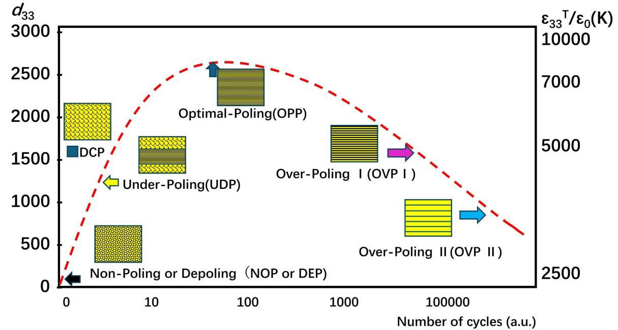
Figure 2. Cycle number dependence of domain structure, dielectric and piezoelectric properties of relaxor-PT SC. Schematic images of domains in NOP (DEP), DCP, UDP, OPP, OVP I and OVP II stages are shown. PT: PbTiO3; SC: single crystal; NOP: non-polarization; DEP: depolarization; DCP: direct-current poling; UDP: under-polarization; OPP: optimum polarization; OVP: over-polarization.
AC poling improves the piezoelectric properties of relaxor single crystals, but the effect is limited in relaxor-PT ceramics[14]. There are two reasons for the smaller increase of the dielectric and piezoelectric properties of the ceramics and textured PMN-PT ceramics when compared to relaxor-PT SCs which show 20%-50% enhancement by ACP. First, the limitation of the domain size in ceramics. From study of SCs, the increase of electrical properties after ACP has been attributed to the change in the domain size. For ceramics sample, the grain size is in the order of 1 to 10 μm, indicating that the domain size must be below these values which cannot be comparable to the domain size in ACP SCs (could be on more than 10 μm). Second, the grains are not exactly along the <001> direction in ceramics, which may lower the enhancement effect of ACP on the electrical properties. It has been reported that ACP does not a large enhancement for the properties for some orientations (e.g., <110>) in relaxor-PT crystals.
The conventional approach for producing relaxor PMN-PT based SCs is the one-charge Bridgeman (OC-BM) growth process. In this method, a compositional gradient of Ti is formed along the length of the OC-BM SC ingot, due to the large segregation coefficient of titanium compared to other elements. Given that the Curie temperature (Tc) and morphotropic phase boundary (MPB) are composition dependent, this variation makes it difficult to maintain uniform physical and electrical properties throughout the length of the OC-BM SC ingot[73-77]. In contrast, the continuous feed BM (CF-BM) growth process developed by JFE Mineral and Alloy Company (JFEM; Chiba, Japan) mitigates Ti segregation by continuously modifying the melt during SC growth and optimizing the platinum crucible speed/feeding rate to achieve synthesis of crystals with enhanced stability[78].
To date, the majority of microstructure observations of DCP and ACP piezoelectric SCs have been conducted using a piezoelectric force microscope (PFM) on areas of less than 20 × 20 μm2. This approach has been employed in numerous studies[9,10,11,15,21,79]. The problem of a small field of view is not sufficient for the evaluation of piezoelectric single crystals, which are not homogeneous through the crystal. SEM, with its ability to zoom in and out of the field of view, is often more effective for observation.
The purpose of this review is to present the relationship between macroscopic/microstructure and piezoelectric properties of DCP and ACP binary and ternary PIN-PMN-PT [001]c SC materials prepared by the BM method using SEM. Furthermore, we will introduce the concept of solid-state crystal growth (SSCG) PMN-PZT SC, which has been the subject of considerable research interest [25,32,80-86].
MATERIALS AND METHODS
Table 1 shows a comparison of domain observation techniques.
Comparison of domain observation techniques
| Field of view (μm) | Object of observation | Merits | Demerits | |
| PFM | 0.1-20 | Electric field induced deformation | High spatial resolution | Limited field of view |
| Dynamic response | ||||
| TEM | 0.1-1 | Morphology | High spatial resolution | Limited field of view |
| Possibility of object change | ||||
| SEM | 5-500 | Morphology | Wide field of view | Difficult to observe dynamically |
| Large depth of focus | ||||
| Optical microscope | 10-1000 | Morphology and optical anisotropy | Dynamic observation | Low resolution |
In PFM, an alternating voltage (excitation voltage) is applied between a short needle at the tip of the cantilever and the sample, and the piezoelectric vibration induced on the sample surface is detected as a deflection (twisting) of the cantilever. This method dynamically visualizes both the magnitude of the change in spontaneous polarization and the phase of the response. It is a very useful technique, but its disadvantage is the limited field of view of 20 × 20 μm of the measurement[9,10,11,15,21,79].
Transmission electron microscopy (TEM) allows for very high-resolution omorphological observations. It is possible to observe fine domain structures that are difficult to detect with scanning electron microscopy or optical microscopy. However, the domain structure may change during sample preparation and observation. The sample for TEM observation must be thin enough to allow the electron beam to penetrate through it, and the sample area must be small enough to fit into the holder. Observation with TEM requires skill, and the results and their interpretation are often affected by the degree of skill. In addition, the electron beam transmitted during observation may alter the arrangement of the domains[87,88].
SEM has a deep depth of focus, which allows a wide range of field of view modification and a large degree of freedom in magnification and reduction. The ability to freely vary the magnification in SEM observations has important implications for the observation of piezoelectric crystals, whose domain structure is heterogeneous within the crystal and whose relative position to the electrode and the direction of application of the electric field are critical. SEM observation captures secondary electrons or reflected electrons when the sample surface is irradiated with electron beams, so the restrictions on sample thickness or area are much smaller than those of TEM. Also, in many cases, the sample is less affected by the electron beam than in TEM. The SEM is used to observe the morphological changes that accompany polarization formation. For this reason, it is necessary to distinguish between microscopic morphology that does not originate from domain structure. In observations of single crystal samples that have been DCP or ACP, the domain structure observed by SEM and PFM is almost the same. He et al. revealed domain structure observed by PFM and SEM is identical[11].
Optical microscopy allows measurements including dynamic observation, and domain observation can be easily performed by using polarized light microscopy[89], but it has the disadvantage of low resolution. Due to the shallow depth of focus of the optical microscope, to obtain such an image, measurements are made by changing the focus and then the image is combined. The actual observed unevenness due to the domain is in the range of 1 mm or less, indicating that it is difficult to observe the sample surface with anything other than SEM if the sample surface is inclined even slightly.
Figure 3 shows (A) equipment for poling process and (B) fractured surface of sliver SC and observation points by SEM. This sample preparation for observation by PFM and SEM is widely used because of the ease of structural observation[22,23]. The sliver shape transducer, (W0.2-0.3 mm, T0.5 mm, and L8-15 mm) are easily broken with a minimum mechanical stress, so it is easy to reveal the fracture surface of SCs by SEM.
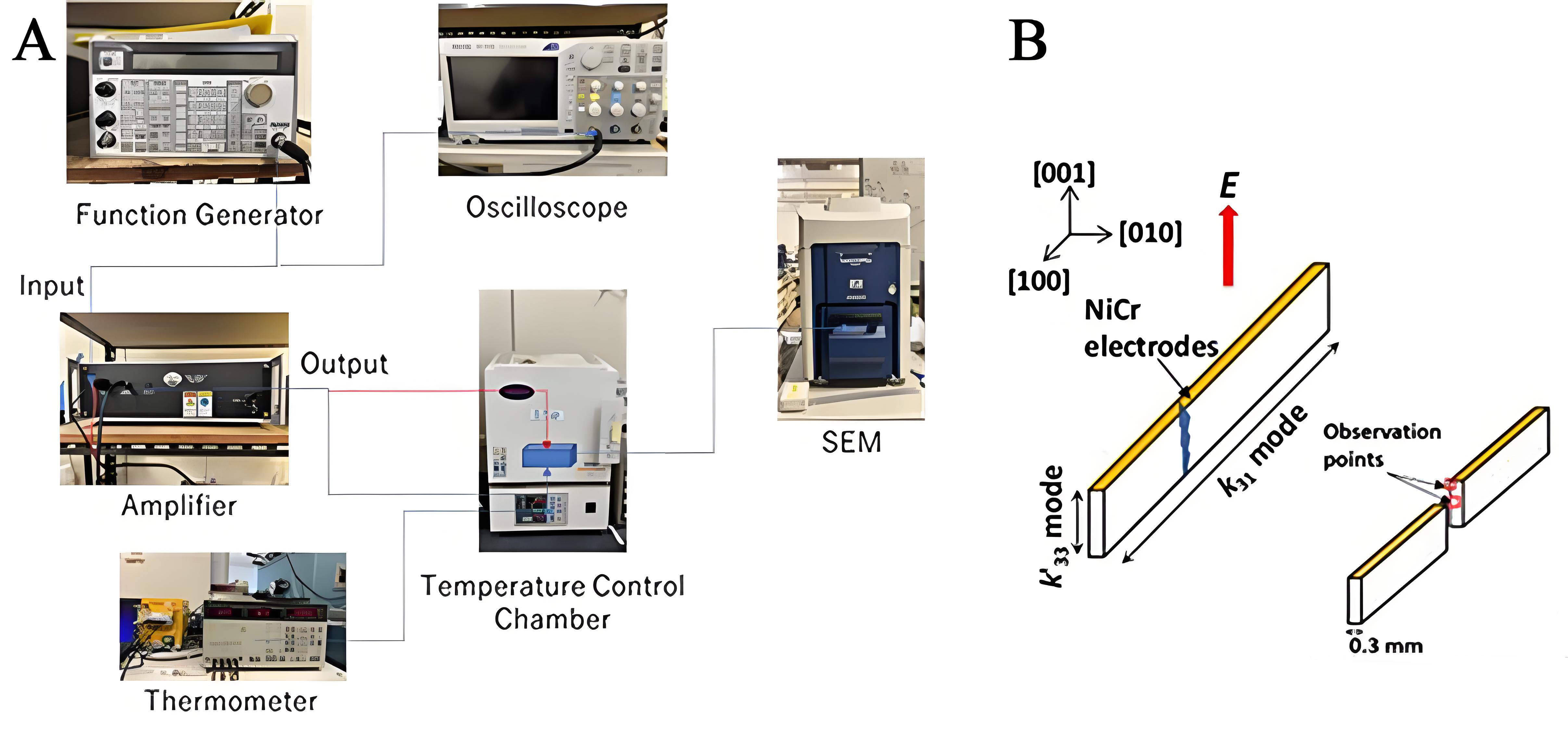
Figure 3. (A) Equipment for poling process; (B) sliver SC sample dimensions, and observation points. SC: Single crystal.
The dielectric constant ε/ε0 of the SC samples was determined from the capacitance at 1 kHz using an impedance analyzer (4194A; Hewlett-Packard Japan). The dielectric loss at that frequency was also measured with the same device. The piezoelectric charge constant of
RESULTS AND DISCUSSION
Microstructure observation of ternary system SCs
In the initial section, we will delineate the microstructure and piezoelectric characteristics of the ternary piezoelectric single crystal 0.24PIN-0.46PMN-0.30PT, which is renowned for its exemplary piezoelectric properties and high-temperature stability. The introduction of the ACP method has led to notable advancements in ternary piezoelectric single crystals, exceeding the achievements of the conventional DCP method. The ACP method enhances piezoelectric and dielectric properties by reinforcing the domain structure within the SC. These enhancements are especially discernible in the vicinity of the MPB, which enables the precise regulation of the material's phase transition to optimize its performance. Piezoelectric materials are utilized across a broad temperature spectrum. Prior research has illustrated the advantages of ACP with respect to both room temperature characteristics and thermal stability, which are crucial for piezoelectric applications operating under diverse temperature regimes[21]. This section will present a comparative analysis of the effects of ACP and DCP on the macro- and microstructures of piezoelectric single crystals, with a view to understand the impact of these structural changes on piezoelectric properties under different temperature conditions.
This section introduces a standard 0.24PIN-0.46PMN-0.30PT ternary piezoelectric single crystal (SC) with [001]c orientation, fabricated using the CF-BM method. This SC exhibits remarkable uniformity in both chemical composition and dielectric and piezoelectric properties. All of the samples of SCs utilized in this experiment were sputtered with electrodes composed of a NiCr/Au (50/200 nm) alloy. In this experiment, an asymmetric sinusoidal wave was employed, with a field of 3.5 to 8 kVrms/cm root mean square (RMS) voltage at 40 °C in air, at a frequency of 0.1 Hz and 22 cycles. Furthermore, DCP was conducted, wherein a field of 8 kV/cm was applied for 60 s in air at 40 °C to facilitate a comparative analysis of the ACP effect exhibited by the SC. Subsequently, a plate of dimensions L13 × W60 × T0.51 mm3 was cut using a dicing saw equipped with a diamond blade (DAD 3350, DISCO Corporation, Tokyo) with a thickness of 0.05 mm. Subsequently, a silver sample with dimensions of L13.0 × W0.3 × T0.51 mm3 was prepared and subjected to ACP treatment for 2, 4, and 8 cycles, respectively, following depolarization treatment at 250 °C.
Figure 4A-D illustrate the polling waveform, DEP SEM image, OPP-DCP SEM image, and OPP-ACP SEM image, respectively. It is noteworthy that the domain size of DEP SC exhibited the finest dimensions, and the SEM morphology was markedly distinct from that of DCP and ACP SC. Figure 4A depicts a schematic representation of the DCP, ACP with 2 to 8 cycles, and 3-step sesquipolar OPP-ACP with 22 cycles[22]. The microstructure of DEP was notably refined, and the OPP-DCP and OPP-ACP SEM images were also of a high degree of fineness. Figure 4C depicts the domain structure of OPP-ACP SCs, wherein 4 striped domains of varying sizes (1-3 μm) were discerned. It was observed that the ACP domains were visibly heterogeneous in size, in comparison to the DEP and DCP domains. It should be noted that certain experimental conditions may have influenced the observed domain structure.
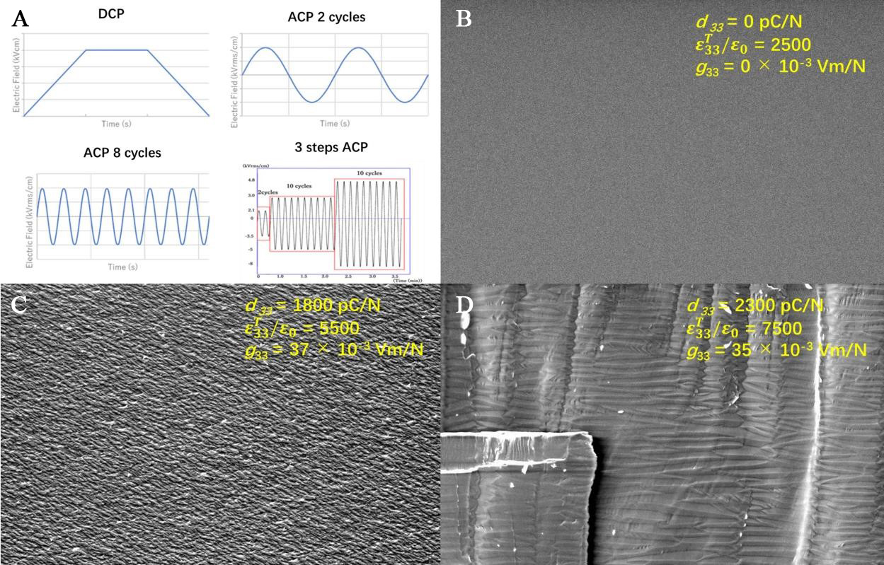
Figure 4. (A) poling wave forms; (B) DEP SEM image; (C) OPP-DCP SEM image; (D) OPP-ACP SEM image. DEP: Depolarization; SEM: scanning electron microscopy; OPP: optimum polarization; DCP: direct-current poling; ACP: alternating-current poling.
Further experiments were conducted. The AC voltage and frequency were fixed at a single value, while the number of cycles was varied from 1 to 1000. The fracture surface was observed using a planar transducer of 3 mm width. Consequently, when the number of cycles was 1, the microstructure exhibited unevenness, whereas when the number of cycles was 10 to 100, it demonstrated relative uniformity. Moreover, upon increasing the number of cycles to 1000, a notable transformation was observed in the microstructure of the fracture surface. Domains with a 109° orientation and a horizontal stripe pattern exceeding 100 μm in length were identified, exhibiting a parallel alignment with the upper and lower electrodes. This indicates that the domains are susceptible to alteration based on the morphology of the sample, the mechanism of fracture, and the prior history, necessitating their consideration when comparing and contrasting.
The fine stripe-like in SC after ACP may contribute to an enhancement of the piezoelectric and dielectric properties. In the SC after DCP, d33 was 1800 pC/N and ε/ε0 = 5500, while in the OPP-ACP SC, d33 was 2300 pC/N and ε/ε0 = 7500. On the other hand, the g33 of DCP and ACP were 37 × 10-3 Vm/N and 35 × 10-3 Vm/N, respectively, and no significant difference was observed. This is due to the fact that both the dielectric constant and d33 increased by the same degree due to the respective poling.
Prior reports have documented the correlation between the number of cycles and the observed characteristics. Wan et al. have reported that the piezoelectric characteristics of PMN-0.26PT SC deteriorate after 100 cycles or more[72]. Furthermore, the dependence of piezoelectric properties on the number of ACP cycles (1, 10, 100, 1,000) and the piezoelectric properties was investigated using a PIN-PMN-PT SC. This result confirms the results of Wan et al. and shows that the piezoelectric properties begin to degrade after about 100 cycles[72]. A schematic diagram is provided in Figure 2. From these results, we can infer that the conventional model of piezoelectric SCs, in which the piezoelectric properties degrade as the domain width increases, is indeed accurate. Furthermore, it can be proposed that relaxor PT SCs may exhibit an optimal domain wall size[91-95].
As illustrated in Figure 5, distinct domain layers were discerned in both DCP and ACP SCs, situated in proximity to the upper and lower electrodes. This result indicates that the different microstructure layers of approximately 20 μm near the upper and lower electrodes are most likely due to the mechanical processing of these SCs, such as lapping and polishing, and/or the electrode formation process, rather than the stress caused by the polarization process. However, this hypothesis still needs to be verified through further investigation.
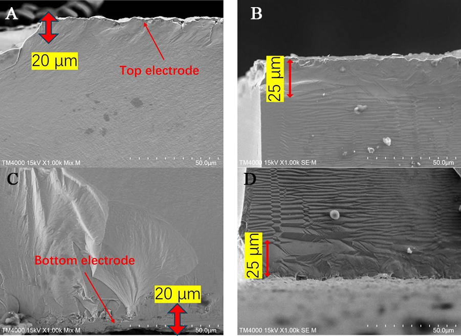
Figure 5. SEM images of (A) OPP-DCP and; (B) OPP-ACP SCs in close proximity to the top (upper images) and bottom (lower images) electrodes. It is notable that in all SCs, there were approximately 20-25 μm of indistinct microstructure layers situated just below these electrodes. SEM: Scanning electron microscopy; OPP: optimum polarization; DCP: direct-current poling; ACP: alternating-current poling; SC: single crystal.
Figure 6 depicts SEM images of DCP SCs following depolarization through heat treatment at 250 °C for 10 min and ACP at 5 kVrms/cm and 0.1 Hz for 2, 4, and 8 cycles. Immediately after depolarization, the SC exhibited an εT33/ε0 value of approximately 2500 and no discernible piezoelectric response was observed in the impedance spectra. Conversely, the εT33/ε0 values after 2, 4, and 8 cycles increased to 1700, 5000, and 6000, respectively, but remained below the optimal ACP SC value of approximately 7,500. This suggests that these samples were not sufficiently polarized, indicating that they were in the UDP stage. The d33 and values of these SCs were lower than 2,300 pC/N of optimal ACP SC. On the other hand, when it comes to the piezoelectric voltage constant g33, it is interesting to note that it is the largest value among these at 2 cycles.
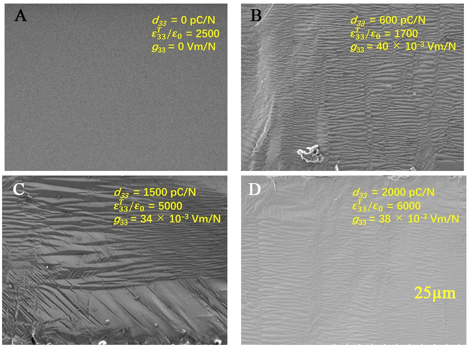
Figure 6. Macro-domain structures and dielectric and piezoelectric properties of SCs (A) DEP after 250 °C heat treatment; (B) UDP-ACP, after (B) 2 cycles; (C) 4 cycles; and (D) 8 cycles. SC: Single crystal; DEP: depolarization; UDP: under-polarization; ACP: alternating-current poling.
The relationship between domain size and piezoelectric properties is believed to be influenced by a number of factors, and a definitive understanding of this relationship remains elusive. It is well established that a reduction in domain size leads to an improvement in the properties of barium titanate (BaTiO3) SCs[91,92]. However, Qiu et al. recently reported that in PMN-0.28PT, the 71° domains disappear in ACP, and the 109° domains show a striped (1-3 μm) structure[15]. Furthermore, Liang et al. recently published a study indicating that a direct comparison of domain sizes between DCP and ACP domains is not a valid approach[29]. In this study, it was found that the piezoelectric properties of ternary SCs deteriorated significantly when 1,000 ACP cycles were applied, and that the 109° domains expanded dramatically in the microstructure. These results suggest that the piezoelectric properties of ternary piezoelectric SCs may degrade as the width of the 109° domain increases.
Let us now provide a brief summary of the results thus far. The differences in the macro- and microstructure of DEP, DCP, and ACP in the rhombohedral 0.24PIN-0.46PMN-0.30PT ternary piezoelectric SC thin plates produced using the CF-BM process were observed using SEM. With the exception of the regions in proximity to the electrodes, the DEP and DCP SCs displayed uniform random domains. However, their dielectric and piezoelectric properties were worse than those of the ACP SC. The ACP SC exhibited four distinct complex domain structures throughout the intermediate UDP and final OPP-ACP stages. In all SC samples, indistinct microstructural regions, potentially resulting from mechanical damage, were recognized in the vicinity of the top and bottom electrodes, which exhibited differences from the crystalline center. Other studies have indicated that the dielectric and piezoelectric properties and electromechanical coupling coefficient of ACP SCs are superior to those of DCP SCs. It is important to note that the domain structure of the piezoelectric SC is heterogeneous even within a plate with a thickness of 0.5 mm. A more detailed and fundamental analysis of the piezoelectric properties and macro- and microstructures of relaxor-PT SCs should be the objective of future research.
Microstructure observation of binary system SCs
The samples utilized in this experiment were PMN-0.28PT SCs fabricated via the conventional OC-BM method. Binary piezoelectric single crystals exhibit the following characteristics: an extremely high mechanical coupling coefficient and piezoelectric constant, high relative permittivity, high transmitting and receiving sensitivity, and a wide bandwidth. The objective of this study was to clarify the relationship between the polarization waveform, microstructure, and piezoelectric properties. As illustrated in Figure 7A, six distinct polarization waveforms were identified. The six types of polarization waveforms are as follows: (a) DCP; (b) pulse DCP; (c) sine ACP; (d) triangle ACP; (e) square ACP; and (f) sawtooth ACP. Sinusoidal ACP, triangular ACP, square ACP, and sawtooth ACP were subjected to an electric field of 1.5 kVrms/cm, a frequency of 0.1 Hz, and 10 cycles at 80 °C in air, as previously described[12]. Pulse DCP was also conducted in accordance with the methodology proposed by Xiong et al.[16]. The pulse DCP conditions were 1.5 kV/cm, 0.1 Hz, and 10 cycles at 80 °C. The standard DCP was conducted at 1.5 kV/cm and 80 °C for a period of 1 min.
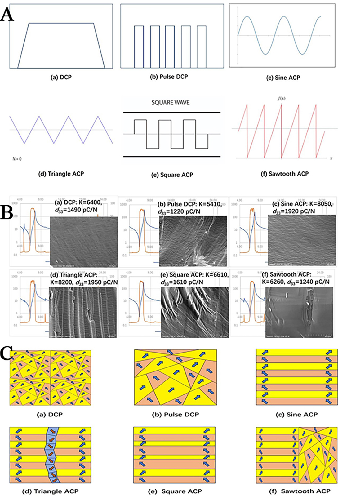
Figure 7. (A) Six poling wave forms; (B) impedance and SEM microstructures; and (C) schematic domain walls images. Copyright from Japanese Journal of Applied Physics[23]. SEM: Scanning electron microscopy.
Figure 7B illustrates the microstructures and piezoelectric properties of the six waveforms under consideration: NOP, pulse DCP, sinusoidal ACP, triangular ACP, square ACP, and sawtooth ACP SC. No discernible 109° domain walls were observed in the pulse DCP samples, and the d33 value was less than 1500 pC/N. In contrast, the sinusoidal ACP SC exhibited 109° domain walls of 1-2 μm in length, aligned with the electrodes, and demonstrated high piezoelectric properties, reaching 1920 pC/N. In this experiment, the sinusoidal ACP SC without spurious-mode vibrations (SMV) exhibited the most stable and optimal electrical properties. Xiong et al. observed that the 109° domain walls were more aligned in the high Tc (280 °C) PIN-0.35PT SC by pulsed poling than in the ACP[16]. However, as illustrated in Figure 7C, in the low-Tc (130 °C) PMN-PT SC utilized in our experiments, the 109° domain structure with a discernible layered configuration was not discerned in the pulsed poling in comparison to the ACP, and was nearly identical to the domain structure obtained by DCP. From these experiments, it can be inferred that 109° domain walls with a moderate width of approximately 0.5 to several micrometers are essential for improving the excellent properties of piezoelectric ACP-based PMN-PT SCs. This conclusion is supported by the findings of previous studies, including those referenced in the following sources: [9,21,22,23].
The pulsed DCP SC exhibited an εT33/ε0 of 5410 and a d33 of 1220 pC/N, both of which were lower than the values observed in the DCP SC, which had an εT33/ε0 of 6400 and a d33 of 1490 pC/N. As illustrated in the schematic domain structure image in Figure 7C[23], the heterogeneity of the constituent phases within the SC plate can be attributed to the heterogeneity of the domain structures. The domain structure images were created with reference to the reports of Qiu et al.[15] and Xiong et al.[16] (a) DCP; (b) pulsed DCP SCs are uniform in phase and exhibit a mixture of 71° and 109° domain structures, as previously reported[15,20,23]; (c) Sinusoidal ACP SCs display striped 109° layers domain walls with 71° domains removed following ACP; (d) Triangular ACP SCs exhibit 109° domain layers similar to those observed in sinusoidal ACP SCs [Figure 7C], but contain irregular domains. As with pulsed DCP, this may be a contributing factor to the SMV; (e) The square ACP SC is analogous to the sinusoidal ACP 109° domain layer in (c), yet the domain layers are not homogeneous in width; (f) serrated ACP SCs exhibit similarities to (c) sinusoidal ACP SC 109° domain layers and also contain domain structures that are reminiscent of those observed in DCP.
In all samples utilized in this study, a substantial microstructure region spanning 20-30 µm was observed directly beneath both electrodes, exhibiting notable dissimilarity from the central region. This finding aligns with the results presented in the preceding section. The disparate microstructures observed directly beneath the electrodes may be attributed to the residual stresses generated during the cutting, grinding, and polishing of the SC plates.
In this study, the observation of microstructure regions with vertical stripes perpendicular to the electrode was consistent for all SCs, despite the application of ACP with different waveforms. This indicates that the presence or absence of the longitudinal stripe microstructure regions in SCs is largely independent of the applied waveform or electric field. Figure 8 illustrates the preparation of SEM samples with two distinct fracture orientations (A) and the SEM microstructures of DCP and sinusoidal ACP PMN-0.28PT SCs with forward and backward bending fracture cross-sections at (B) low and (C) high magnifications. As illustrated in the SEM images, the location of the longitudinal stripe region of the SC plate changes with the fracture direction in the case of DCP SC, even when the applied electric field remains constant. In contrast, the position of the longitudinal stripe region remains consistent for the same fracture direction in the case of the sine ACP SC. These findings suggest that when a DCP or ACP SC is fractured, a microstructure with longitudinal striations perpendicular to the direction of tensile stress application is formed. As previously reported, the use of SC slivers with a width less than half the thickness and a length perpendicular to the electrode direction (e.g., L13 × W0.15 × T0.3 mm) has been shown to result in a good fracture surface, thereby reducing tensile stress[23]. As reported by Song et al. the SEM image of PIN-PMN-PT SC reveals the presence of a microstructure of longitudinal stripes perpendicular to the electrode[95]. However, the authors did not explicitly discuss the formation of this microstructure in relation to the different fracture directions.
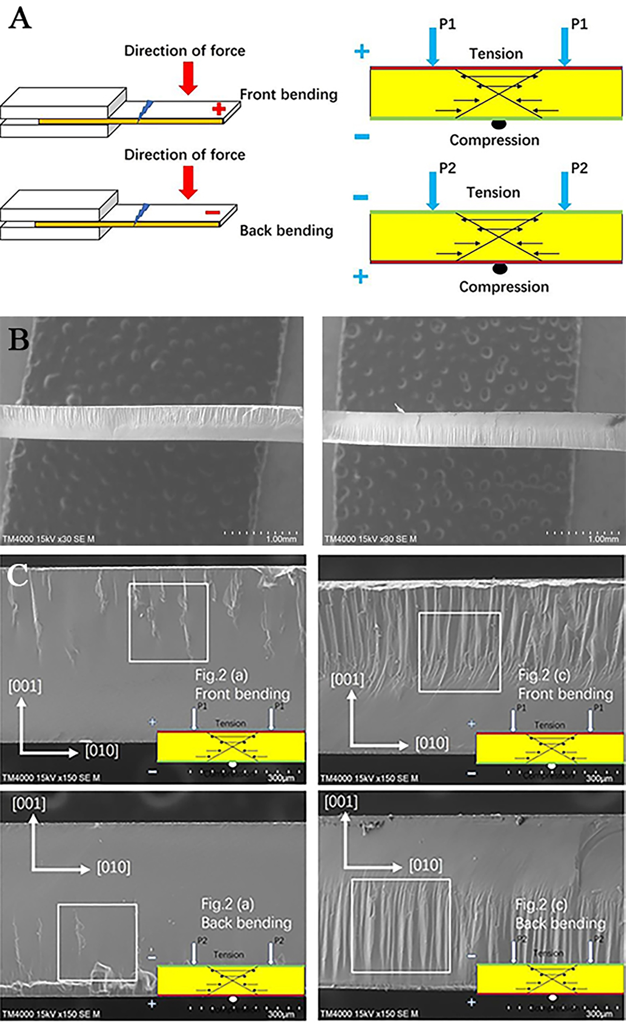
Figure 8. (A) Two SEM specimen preparation methods in different fracture directions and, SEM microstructures of anterior and posterior bending fracture surfaces at (B) low and (C) high magnifications. SEM: Scanning electron microscopy.
In contrast, as illustrated in Figure 8, our findings indicate that the location of the longitudinal stripe microstructure shifts in PMN-PT SC due to the discrepancy in compression and tension resulting from the distinction in fracture direction. The longitudinal stripe microstructure is the result of a distinct formation process influenced by the intrinsic domain structure of the piezoelectric material. Consequently, when employing SEM to examine the microstructure of SCs and elucidate the correlation between piezoelectric properties, it is imperative to prioritize meticulous sample preparation and precise observation geometry.
Various theories have been proposed and reported by many researchers on the mechanism of enhancement of piezoelectric properties by ACP of piezoelectric SCs[8,11,15,21]. Wada et al. reported that in barium titanate SC, small domain walls, i.e., high domain wall density, exhibit high piezoelectric property[91,92]. Yamamoto et al. reported that the optimal domain wall width for ACP SCs is about 0.5 to 5 μm with stripes of 109° parallel to the electrode[6]. ACP SCs also showed a clear change in the [004] peak observed by X-ray diffraction (XRD), indicating not only a change in the domain but also a change in the constituent phases[6,7]. Qiu et al. reported that the reduction of 71° domain walls and the increase in domain size of ACP single crystals caused transparency, which is the main reason for the improved piezoelectric properties[15]. Wan et al. and Xiang et al. reported that excessive cyclic ACP poling conditions for PMN-PT SCs lead to large 109° domain wall widths, which degrade the piezoelectric properties, and that there is an optimal domain wall width[23,72].Tian et al. proposed that ACP causes lattice defects in single crystals to accumulate around 109 domain walls, which is responsible for the excellent piezoelectric properties[24].
Liang et al. reported the presence of new sub-1 μm fine 71° stripe domains in 109° domain walls parallel to the polarization direction after thermal cycling of ACP PMN-PT single crystals at 60 °C, and since there is little change in the dielectric piezoelectric properties of SCs before and after this heat treatment, they report that they do not believe that the bigger the domain, the better[29]. We believe that the improvement in the piezoelectric properties of PMN-PT piezoelectric SCs by ACP is not only due to the change in the microstructure of less than 5 μm, but also due to the machined layer of about 25 μm macrostructure at the bottom of the electrode, which greatly affects the electrical properties of the SCs plates. This idea is supported by the results reported by Kim et al. who found little property enhancement effect of ACP when the thickness of single crystals is less than 100 μm[18]. Sato reported that the MPB PMN-PT SC was examined using in situ AC field electrical biasing transmission electron microscopy. The ferroelectric domain structure was significantly altered by applying a SC of an AC electric field at 12 kV/cm peak-to-peak (3.6 kVrms/cm) and 20 Hz. Subsequently, with increased AC field duration, both a reduction in domain wall density and the generation of vertical microdomain bands were observed. These phenomena could, respectively, enhance and degrade the piezoelectricity of the material[87].
PMN-PT SCs near morphotropic phase boundaries with excellent piezoelectric properties have complex compositions, domains and multiple constituent phases, and these properties are easily changed by physical and electrical stimuli. It is not yet clear which factors are responsible for the enhanced properties of ACP PMN-PT piezoelectric SCs and to what extent, and further research is needed.
Solid state crystal growth (SSCG)
Figure 9 shows (A) a schematic fabrication image of the SSCG process, (B) the 0-12 MHz impedance spectrum of a high-Qm SSCG SC without the poling process, (C) a low-density type, (D) a high-density type SSCG SC, and (E) an SEM of a PIN-PMN-PT BM SC after ACP images and piezoelectric properties[25]. SSCG technology has been studied since the 1990s as a fabrication method for Mn-Zn ferrite and garnet. SSCG is a method of growing SCs from polycrystals in the solid phase and is based on Abnormal Grain Growth (AGG) in solid phase reactions. Seed crystals are embedded in or placed on top of the polycrystalline body. The seed crystal has the same crystalline structure as the matrix material. Both the seed SC and the polycrystal are sintered at a temperature below the melting point of the crystal to form an SC material from the polycrystal. In addition, SCs can be grown using the “seed-free method” by nucleating seed crystals in the polycrystalline matrix in advance by applying a temperature gradient or by adding additive materials such as boron (B2O3). SSCG has long been used as a low-cost method for producing SC materials, but it has only recently attracted attention. The SSCG process offers some advantages: (1) Heating equipment can be easily designed to grow at lower temperatures than the melt growth method; (2) Composition uniformity is good because segregation is less likely to occur; (3) Crucible contamination is suppressed. Many of the problems associated with conventional SC growth can be avoided with the SSCG method, and there are prospects for lower production costs. The so-called BM furnace used in the BM method is a special piece of equipment. However, the equipment used in SSCG SC can be a general-purpose electric furnace for sintering ceramics, and the use of a continuously operating furnace called a tunnel furnace enables mass production at lower cost. When heterogeneous nucleation starts on the surface of a relaxor-based piezoelectric SC with a seed crystal [Ba(Ti,Zr)O3 with a perovskite structure], atom diffusion occurs from the high-density ceramic matrix to the seed crystal in contact. As a result, abnormal grain growth (AGG) is activated and crystals can be grown epitaxially from the seed crystal. The SSCG method has several advantages: the production of relaxor-based piezoelectric SCs by the SSCG method does not require a high-cost platinum (Pt) or iridium (Ir) crucible, which is a prerequisite for the BM method, because SC growth is performed in a sealed porcelain sager, typically at 1100 °C to 1250 °C. Therefore, the SSCG method can also significantly reduce manufacturing costs. In addition to the economic aspect, the homogeneous composition throughout the volume of the SC is ensured because the raw ceramic powder is not melted. Currently, compositional variations within SSCG SCs are known to be in the range of ± 0.25 mol%, which is similar to commercialized PZT ceramics and barium titanate, resulting in excellent uniformity and reproducibility of electrical properties[25]. It is noteworthy that with the advantage of guaranteed uniformity, the amounts of donors (Sm, Nd, La, W, etc.) and acceptors (Fe, Mn, Co, etc.) can be easily adjusted, resulting in convenient control of the dielectric and piezoelectric properties. One feasible method that has received particular attention is the inclusion of a self-activated poling state, or self-poling, by adding additives to the relaxor PT SC. He et al. reported the self-poling properties of top-seeded solution-grown (TSSG) Sn-doped PMN-PIN SCs, d33 > 1500 pC/N in 2017[96]. We demonstrated that SSCG PMN-PZT SCs exhibited large d33 > 540 pC/N[25]. Kim et al. also reported self-polling of SSCG PMN-PZT,
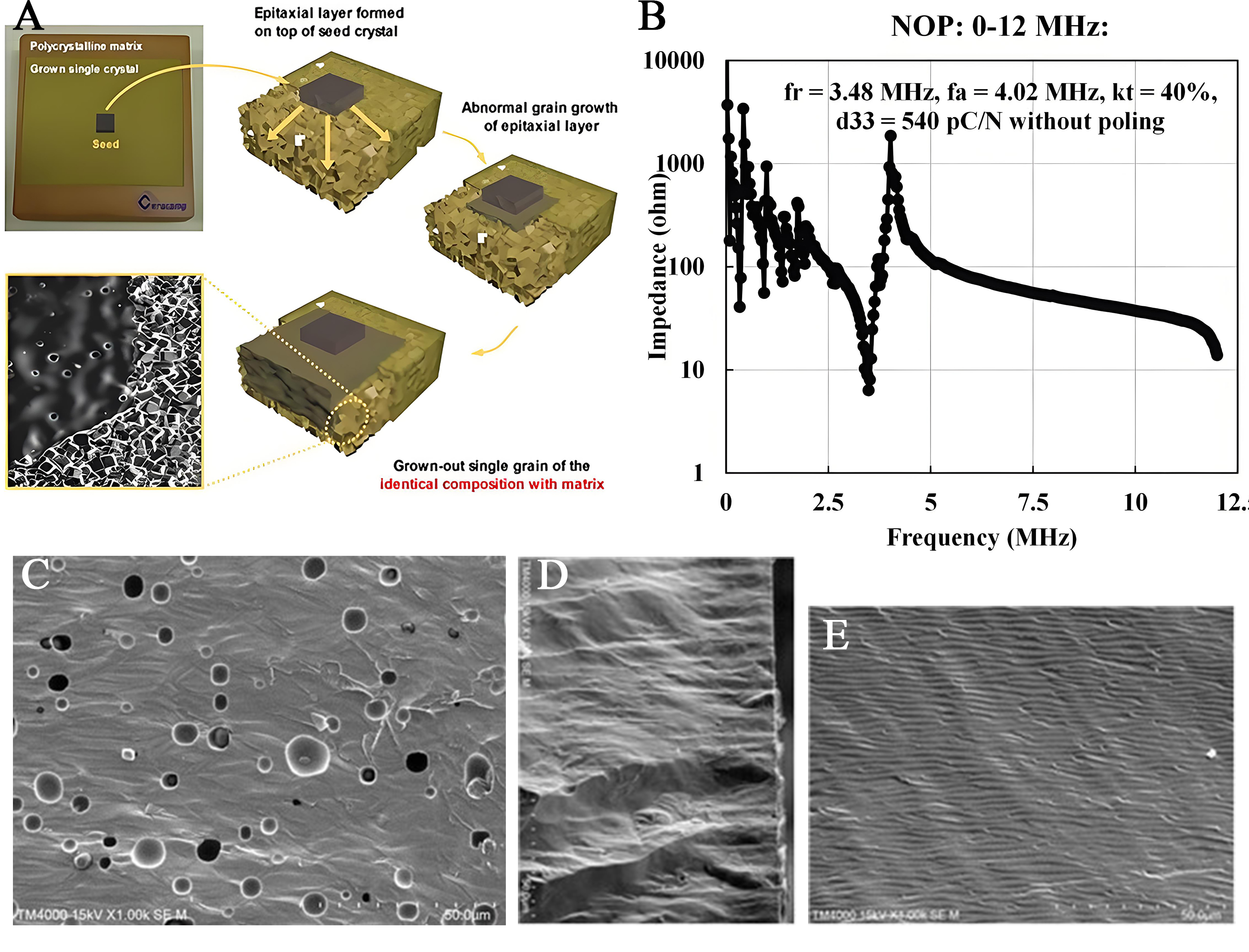
Figure 9. (A) Production image of SSCG process, (B) Impedance spectra of NOP SC with 0-12 MHz, for high Qm SSCG SC without any poling process. Copyright from Japanese Journal of Applied Physics[25]; (C) SEM images of low-density-type. Copyright from Japanese Journal of Applied Physics[32]; (D) high-density type SSCG SC; and (E) PIN-PMN-PT BM SCs after ACP. Copyright from Japanese Journal of Applied Physics[80]. SSCG: Solid-state crystal growth; NOP: non-polarization; SC: single crystal; ACP: alternating-current poling; BM: Bridgeman method; PIN: Pb(In1/2Nb1/2)O3; PT: PbTiO3; PMN: Pb(Mg1/3Nb2/3)O3
where Z2 is the acoustic impedance of the piezoelectric body and Z1 is the acoustic impedance of the living body. At Z2 values of 28 MRayls and 35 MRayls, the reflectance rates are measured to be 89.8% and 91.8%, respectively. Correspondingly, the transmittance values are 10.2% and 8.2%, indicating a difference of 20% at this point. In actual applications, acoustic impedance matching layers are often incorporated into the design of the actual transducer, which is located between the living body and the piezoelectric material. However, as the above analysis clearly shows, even a 20% improvement in acoustic impedance can have a very significant effect on performance improvement and generate significant industrial value. In addition to these, SSCG crystals have excellent machinability because crack propagation is inhibited by the presence of pores. For these reasons, SSCG SCs have the potential to be a game changer for various piezoelectric transducers in the near future[80]. Table 2 shows a comparison of DCP and ACP material constants for low-density SSCG, high-density SSCG, and CF-BM grown PIN-PMN-PT SCs.
Comparison of material constants of low-density (LD) SSCG, high-density (HD) SSCG, and CF-BM growth PMN-PT SCs. Copyright from Japanese Journal of Applied Physics[25].
| Properties/Materials | LD SSCG PMN-0.3PT | HD SSCG PMN-0.3PZT | CF-BM PMN-0.30PT | ||||
| Density (g/cm3) | 7.5 | 7.5 | 7.8 | 7.8 | 8.11 | 8.11 | |
| Poling type | DCP | ACP | DCP | ACP | DCP | ACP | |
| Free dielectric constant | 5200 | 6,450 | 10,000 | 14,200 | 6,000 | 10,000 | |
| Clamped dielectric constant | 1,030 | 1,000 | 1,000 | 1,250 | 815 | 770 | |
| Dielectric loss (%) | 0.8 | 0.9 | 1.1 | 1.2 | 0.5 | 0.4 | |
| Calculated k33 (%) | 90 | 92 | 95.4 | 95.7 | 92.8 | 96.1 | |
| kt (%) | 59.1 | 58 | 47 | 48.2 | 56.7 | 56.5 | |
| Nt (Hz•m) | 1,750 | 1,770 | 1,980 | 2,000 | 1,918 | 1,920 | |
| Sound velocity (m/sec.) | 4,025 | 4,100 | 4,450 | 4,490 | 4,560 | 4,635 | |
| d33 (pC/N) | 1,330 | 1,530 | 2,800 | 4,800 | 1,600 | 3,000 | |
| g33 (10-3 Vm/N) | 28.9 | 26.8 | 31.6 | 38.2 | 30.1 | 33.9 | |
| Acoustic impedance Z33 (MRayls) | 30.2 | 30.8 | 34.7 | 35.0 | 37.0 | 37.6 | |
| Coercive field Ec (kV/cm) | 3.0 | 3.0 | 3.0 | 3.0 | 2.5 | 2.4 | |
| Tpc1 (°C) | 80 | 74 | 57 | 58 | 88 | 87 | |
| Tpc2 (°C) | 86 | 72 | 72 | 98 | |||
| Tc (°C) Max. dielectric loss | 109 | 114 | 140 | 140 | 141 | 141 | |
| Tm (°C) Max. dielectric constant | 117 | 119 | 148 | 148 | 143 | 143 | |
However, the practical application of SSCG-PMN-PT based SCs still lags behind BM process SCs, which have been developed in many research periods and companies since the 1990s; the SSCG method has difficulties in stably controlling pore size and pore volume, stably producing SCs larger than 70 mm in length and weighing more than 0.5 kg[81-84]. There are few research institutes, and the number of product suppliers is limited to one company worldwide[86]. Therefore, more active research and development is needed for the large-scale application of SSCG SC in the near future.
CONCLUSIONS
The use of AC poling instead of conventional DC poling to improve the properties of high-performance relaxor perovskite piezoelectric SCs produced by the Bridgeman melt-growth method has become common since about 2020. The microstructure of relaxor PT SCs is easily modified by machining, polishing, lapping processes, electrode attachment, electric fields, and mechanical stress. Microstructural observation by scanning electron microscopy SEM is the best way to easily confirm the relationship between electrical properties, macrostructure, and microstructure of relaxor-PbTiO3 SCs.
After optimal AC poling, a fine 109o domain layer of 0.5 to several microns is obtained parallel to the electrodes of the relaxor-PbTiO3 SC plate, which contributes to a 10%-100% improvement in the dielectric constant and piezoelectric constant. Selection of the proper voltage, waveform, and the optimum number of AC cycles (5-200 cycles) are necessary to obtain stable electrical properties.
Non-melt growth type relaxor-based piezoelectric SCs fabricated by the SSCG method exhibit self-poling, excellent machinability, high piezoelectric performance, and excellent composition uniformity, which is attributed to the spherical micropores present in the SCs. However, further improvements are needed for SSCG SCs to become the mainstay of future applications. The AC poling technology can be applied not only to lead-based relaxor piezoelectric SCs but also to other lead-free piezoelectric SCs and ceramics. Further research is needed, including theoretical aspects, for the wider application of AC poling.
DECLARATIONS
Acknowledgments
Authors express our sincerely acknowledgments to Prof. Xiaoning Jiang, Drs. Sipan Liu, Zengege Xu of NC state university NC, USA, Dr. Tomoaki Karaki, Dr. Yiqin Sun of ex-Toyama prefectural university, Toyama, Japan for useful discussion.We thank Mr. K-Echizenya of JFE Mineral and Alloy Co. Japan and Mr. H. Kubota, Mr. Kitahata of Tayca Corp. Japan for single crystal sample preparation and useful discussion.
Authors’ contributions
Experiment, characterization, writing original draft: Xiang, Y.; Maiwa, H.
Review & editing, supervision: Lee, H. Y.
Methodology and sample preparation: Lee, H. Y.; Xiang, Y.
High-resolution SEM: Xiang, Y.; Sun, Y.
Conceptualization, review, supervision: Yamashita, Y.
Availability of data and materials
According to reasonable requirements, all of the data examined in this research can be obtained from the correspondents.
Financial support and sponsorship
This work was supported by the Murata Science Foundation (Grant No. 2023-001),
Conflicts of interest
Lee, H. Y. is affiliated with Ceracomp Co., Ltd.. The other authors have declared that they have no conflicts of interest.
Ethical approval and consent to participate
Not applicable.
Consent for publication
The person in Figure 1C is one of the co-authors, Yohachi Yamashita, and we have obtained permission to publish his image.
Copyright
© The Author(s) 2025.
REFERENCES
1. Park, S. E.; Shrout, T. Characteristics of relaxor-based piezoelectric single crystals for ultrasonic transducers. IEEE. Trans. Ultrason. Ferroelect. Freq. Contr. 1997, 44, 1140-7.
2. Rehrig, P. W.; Hackenberger, W. S.; Jiang, X.; Shrout, T. R.; Zhang, S.; Speyer, R. Status of piezoelectric single crystal growth for medical transducer applications. In 2003 IEEE Symposium on Ultrasonics, Proceeding of 2003 IEEE Ultrasonics Symposium, Honolulu, HI, USA, October 5-8, 2003; Yuhas, D. E., Susan C. Schneider, S. C., Eds; IEEE: Piscataway, New Jersey, USA, 2003; Vol. 1, pp 766-9.
3. Zhang, S.; Li, F. High performance ferroelectric relaxor-PbTiO3 single crystals: Status and perspective. J. Appl. Phys. 2012, 111, 031301.
4. Zhang, S.; Li, F.; Yu, F.; et al. Recent Developments in Piezoelectric Crystals. J. Korean. Ceram. Soc. 2018, 55, 419-39.
5. Uchino, K. Electrostrictive and piezoelectric effects in relaxor ferroelectrics: historical background. IEEE. Trans. Ultrason. Ferroelectr. Freq. Control. 2022, 69, 3013-36.
6. Yamamoto, N.; Yamashita, Y.; Hosono, Y.; Itsumi, K.; Higuchi, K. Ultrasonic probe, piezoelectric transducer, method of manufacturing ultrasonic probe, and method of manufacturing piezoelectric transducer. US20140062261A1, 2014.
7. Yamashita, Y.; Yamamoto, N.; Hosono, Y.; Itsumi, K. Piezoelectric transducer, ultrasonic probe, and method of manufacturing piezoelectric transducer. US20150372219A1, 2015.
8. Xu, J.; Deng, H.; Zeng, Z.; et al. Piezoelectric performance enhancement of Pb(Mg1/3Nb2/3)O3-0.25PbTiO3 crystals by alternating current polarization for ultrasonic transducer. Appl. Phys. Lett. 2018, 112, 182901.
9. Chang, W.; Chung, C.; Luo, C.; et al. Dielectric and piezoelectric properties of 0.7 Pb(Mg1/3Nb2/3)O3 -0.3 PbTiO3 single crystal poled using alternating current. Mater. Res. Lett. 2018, 6, 537-44.
10. Wan, H.; Luo, C.; Chang, W.; Yamashita, Y.; Jiang, X. Effect of poling temperature on piezoelectric and dielectric properties of 0.7Pb(Mg1/3Nb-)O3-0.3PbTiO3 single crystals under alternating current poling. Appl. Phys. Lett. 2019, 114, 172901.
11. He, C.; Karaki, T.; Yang, X.; Yamashita, Y.; Sun, Y.; Long, X. Dielectric and piezoelectric properties of
12. Sun, Y.; Karaki, T.; Fujii, T.; Yamashita, Y. Alternate current poling and direct current poling for Pb(Mg1/3Nb2/3)O3-PbTiO3 single crystals. Jpn. J. Appl. Phys. 2019, 58, SLLC06.
13. Luo, C.; Wan, H.; Chang, W.; et al. Effect of low-frequency alternating current poling on 5-mm-thick 0.7Pb(Mg1/3Nb2/3)O3-0.3PbTiO3 single crystals. Appl. Phys. Lett. 2019, 115, 192904.
14. Yang, S.; Wang, M.; Wang, L.; et al. Achieving both high electromechanical properties and temperature stability in textured PMN-PT ceramics. J. Am. Ceram. Soc. 2022, 105, 3322-30.
15. Qiu, C.; Wang, B.; Zhang, N.; et al. Transparent ferroelectric crystals with ultrahigh piezoelectricity. Nature 2020, 577, 350-4.
16. Xiong, J.; Wang, Z.; Yang, X.; Long, X.; He, C. Optimizing the piezoelectric and dielectric properties of Pb(In1/2Nb1/2)O3-PbTiO3 ferroelectric crystals via alternating current poling waveform. IEEE. Trans. Ultrason. Ferroelectr. Freq. Control. 2021, 68, 2775-80.
17. Deng, C.; Ye, L.; He, C.; et al. Reporting excellent transverse piezoelectric and electro-optic effects in transparent rhombohedral PMN-PT single crystal by engineered domains. Adv. Mater. 2021, 33, e2103013.
18. Kim, H. P.; Wan, H.; Lu, X.; Yamashita, Y.; Jiang, X. Scaling effects in the alternating-current poling of thin PIN-PMN-PT single crystals. Appl. Phys. Lett. 2022, 120, 142901.
19. Sun, Y.; Ota, Y.; Fujii, T.; et al. Enhanced properties of 3-MHz sliver-mode vibrators for cardiac probes with alternating current poling for Pb(Mg1/3Nb2/3)O3-PbTiO3 single crystals. IEEE. Trans. Ultrason. Ferroelectr. Freq. Control. 2022, 69, 3087-94.
20. Kim, H. P.; Wan, H.; Luo, C.; et al. A review on alternating current poling for perovskite relaxor-PbTiO3 single crystals. IEEE. Trans. Ultrason. Ferroelectr. Freq. Control. 2022, 69, 3037-47.
21. Yamashita, Y.; Karaki, T.; Lee, H. Y.; Wan, H.; Kim, H. P.; Jiang, X. A review of lead perovskite piezoelectric single crystals and their medical transducers application. IEEE. Trans. Ultrason. Ferroelectr. Freq. Control. 2022, 69, 3048-56.
22. Xiang, Y.; Sun, Y.; Yamashita, Y.; Karaki, T.; Maiwa, H. Macro- and microstructure of lead perovskite ternary piezoelectric single crystals after direct current and alternating current poling. J. Ceram. Soc. Japan. 2023, 131, 263-9.
23. Xiang, Y.; Sun, Y.; Yamashita, Y.; Karaki, T.; Maiwa, H. Microstructure observation of Pb(Mg1/3Nb2/3)O3-PbTiO3 single crystals by scanning electron microscopy. Jpn. J. Appl. Phys. 2023, 62, SM1029.
24. Tian, G.; Liu, F.; Du, J.; et al. Simultaneous enhancement of piezoelectricity and mechanical quality factor in relaxor-ferroelectric crystals via defect engineering. Appl. Phys. Lett. 2023, 122, 102901.
25. Maiwa, H.; Yamagata, Y.; Xiang, Y.; Sun, H.; Lee, H.; Yamashita, Y. Self-poling and DC poling of Mn doped Pb(Mg1/3Nb2/3)O3-Pb(ZrTi)O3 single crystals grown by a solid state crystal growth process. Jpn. J. Appl. Phys. 2024, 63, 04SP50.
26. Wu, H.; Han, S.; Liu, J.; et al. Enhanced high-power behaviors of Mn-doped Pb(In1/2Nb1/2)O3-Pb(Mg1/3Nb2/3)O3-PbTiO3 piezoelectric crystals through combining direct and alternating current polarization. J. Alloys. Compd. 2024, 989, 174370.
27. Kumar, A.; Kim, W.; Sriboriboon, P.; Lee, H.; Kim, Y.; Ryu, J. AC poling-induced giant piezoelectricity and high mechanical quality factor in [001] PMN-PZT hard single crystals. Sensors. Actuat. A:. Phys. 2024, 372, 115342.
28. Wang, S.; Liu, Z.; Han, L.; et al. Mesophase induced by alternating-current poling in relaxor ferroelectric single crystals. Acta. Materialia. 2024, 268, 119782.
29. Liang, M.; Xiong, R.; Chen, S.; et al. Thermal cycle stability and microstructure of Pb(Mg1/3Nb2/3)O3-PbTiO3 single crystals. J. Appl. Phys. 2024, 135, 164104.
30. Li, F.; Wang, B.; Chen, L. Phase-field-guided design of record-high piezoelectricity and discovery of simultaneous high light transparency and high piezoelectricity in relaxor ferroelectrics. MRS. Bulletin. 2024, 49, 626-35.
31. Kim, H. P.; Zhang, M. H.; Wang, B.; Wu, H.; Moon, S.; Xu, Z.; et al. Electrical de-poling and re-poling of relaxor-PbTiO3 piezoelectric single crystals without heat treatment. Nature commun 2024. p. 6420.
32. Maiwa, H.; Yamagata, Y.; Xiang, Y.; Lee, H.; Yamashita, Y. AC poling of high Qm and low acoustic impedance Pb(Mg1/3Nb2/3)O3-Pb(Zr,Ti)O3 single crystals produced by a solid-state crystal growth. Jpn. J. Appl. Phys. 2024, 63, 10SP01.
33. Qiu, C.; Liu, J.; Li, F.; Xu, Z. Thickness dependence of dielectric and piezoelectric properties for alternating current electric-field-poled relaxor-PbTiO3 crystals. J. Appl. Phys. 2019, 125, 014102.
34. Zhang, Z.; Xu, J.; Yang, L.; et al. The performance enhancement and temperature dependence of piezoelectric properties for
35. Kim, S.; Khanal, G. P.; Nam, H.; Fujii, I.; Ueno, S.; Wada, S. Effects of AC- and DC-bias field poling on piezoelectric properties of Bi-based ceramics. J. Ceram. Soc. Japan. 2019, 127, 353-6.
36. Zhou, Y.; Li, Q.; Zhuo, F.; et al. Domain switching and polarization fatigue in rhombohedral PIN-PMN-PT and Mn-doped
37. Lee, G.; Kim, H.; Lee, S.; Lee, H.; Jo, W. Depolarization mechanism of alternating-current-poled Pb(Mg1/3Nb2/3)O3-PbTiO3 single crystals measured using in-situ thermally stimulated depolarization current. KSS. 2020, 29, 59-62.
38. Ma, M.; Xia, S.; Song, K.; Guo, H.; Fan, S.; Li, Z. Enhanced dielectric and piezoelectric properties in the [001]-poled
39. Guo, L.; Su, B.; Wang, C.; et al. Orientation dependence of dielectric and piezoelectric properties of tetragonal relaxor ferroelectric single crystals by alternate current poling. J. Appl. Phys. 2020, 127, 184104.
40. Jiang, Z.; Ye, Z. Application study of Mn-doped PIN-PMN-PT relaxor ferroelectric crystal grown by vertical gradient Freeze method. Ferroelectrics 2020, 557, 9-17.
41. Xu, J.; Zhang, Z.; Liu, S.; et al. Optimizing the piezoelectric vibration of Pb(Mg1/3Nb2/3)O3-0.25PbTiO3 single crystal by alternating current polarization for ultrasonic transducer. Appl. Phys. Lett. 2020, 116, 202903.
42. Liu, J.; Qiu, C.; Qiao, L.; et al. Impact of alternating current electric field poling on piezoelectric and dielectric properties of
43. Ma, J.; Zhu, K.; Huo, D.; Qi, X.; Sun, E.; Zhang, R. Performance enhancement of the piezoelectric ceramics by alternating current polarizing. Appl. Phys. Lett. 2021, 118, 022901.
44. Ma, M.; Xia, S.; Song, K.; Guo, H.; Xu, Z.; Li, Z. Temperature dependence of the transverse piezoelectric properties in the [001]-poled 0.25Pb(In1/2Nb1/2)O3-0.42Pb(Mg1/3Nb2/3)O3-0.33PbTiO3 single crystal with alternating current treatment. J. Appl. Phys. 2021, 129, 114102.
45. Hong, C.; Wang, Z.; Su, B.; et al. Enhanced piezoelectric and dielectric properties of Pb(Yb1/2Nb1/2)O3-Pb(Mg1/3Nb2/3)O3-PbTiO3 crystals by combining alternating and direct current poling. J. Appl. Phys. 2021, 129, 124101.
46. Xiong, J.; Wang, Z.; Yang, X.; Su, R.; Long, X.; He, C. Effects of alternating current poling on the dielectric and piezoelectric properties of Pb(In0.5Nb0.5)O3-PbTiO3 crystals with a high Curie temperature. RSC. Adv. 2021, 11, 12826-32.
47. Qiu, C.; Xu, Z.; An, Z.; et al. In-situ domain structure characterization of Pb(Mg1/3Nb2/3)O3-PbTiO3 crystals under alternating current electric field poling. Acta. Materialia. 2021, 210, 116853.
48. Ma, J.; Zhu, K.; Huo, D.; et al. Performance enhancement of 1-3 piezoelectric composite materials by alternating current polarising. Ceram. Int. 2021, 47, 18405-10.
49. Liao, F.; Zhao, Y.; Chen, Z.; Zheng, Y.; Chen, H. Bridgman growth and photoelectronic property of relaxor-based ferroelectric single crystal Pb(Sm1/2Nb1/2)O3-Pb(Mg1/3Nb2/3)O3-PbTiO3. Crystals 2021, 11, 402.
50. Ushakov, A. D.; Hu, Q.; Liu, X.; Xu, Z.; Wei, X.; Shur, V. Y. Domain structure evolution during alternating current poling and its influence on the piezoelectric properties in [001]-cut rhombohedral PIN-PMN-PT single crystals. Appl. Phys. Lett. 2021, 118, 232901.
51. Long, W.; Fan, X.; Fang, P.; Li, X.; Xi, Z. Optical Properties and Band Gap of Ternary PSN-PMN-PT Single Crystals. Crystals 2021, 11, 955.
52. Deng, T.; Fang, B.; Di, W.; et al. Electrical performance and ferroelectric phase transition characteristic in different oriented
53. Xiong, J.; Wang, Z.; Yang, X.; Su, R.; Long, X.; He, C. Impact of thickness and poling condition on dielectric and piezoelectric properties of Pb(In0.5Nb0.5)O3-PbTiO3 ferroelectric crystals. Physica. Status. Solidi. (b). 2022, 259, 2100287.
54. Chen, Z.; Deng, T.; Chen, R.; et al. Bridgman growth and electrical properties of Nd-doped PMN-PT single crystal with ultrahigh piezoelectricity. CrystEngComm 2022, 24, 837-45.
55. Baasandorj, L.; Chen, Z. Recent developments on relaxor-PbTiO3 ferroelectric crystals. Crystals 2022, 12, 56.
56. Jing, Y.; Liu, F.; Qi, X.; et al. Property enhancement in relaxor-PbTiO3 single crystals by alternating current poling: evaluation of intrinsic and extrinsic contributions. Ceram. Int. 2022, 48, 11764-71.
57. Liu, M.; Tang, H.; Zhang, W.; et al. Complete sets of material constants of [001]-poled 0.72Pb(Mg1/3Nb2/3)O3-0.28PbTiO3 single crystals using alternating current poling. IEEE. Trans. Ultrason. Ferroelectr. Freq. Control. 2022, 69, 3081-6.
58. Ma, M.; Xia, S.; Gao, X.; et al. Enhanced energy harvesting performance of PIN-PMN-PT single crystal unimorph using alternating current poling. Appl. Phys. Lett. 2022, 120, 042902.
59. Kong, S.; Hong, C.; Zhang, W.; et al. Performance enhancement of soft-PZT5 piezoelectric ceramics using poling technique. J. Am. Ceram. Soc. 2022, 105, 4744-50.
60. Xiong, J.; Wang, Z.; Yang, X.; et al. Performance enhancement of Pb(In1/2Nb1/2)O3-PbTiO3 ferroelectric single crystals using pulse poling. Scripta. Materialia. 2022, 215, 114694.
61. Nozaki, T.; Martin, A.; Kobayashi, R.; Nakayama, T.; Kakimoto, K. Pulse-poling and characterization of (Na,K)NbO3 ceramics. Jpn. J. Appl. Phys. 2022, 61, SN1030.
62. Ma, J.; Huo, D.; Qi, X.; et al. Enhanced electromechanical properties in Pb(Mg1/3Nb2/3)O3-PbTiO3 based 1-3 piezoelectric composites using the alternating current poling method. Mater. Sci. Eng:. B. 2022, 284, 115890.
64. Kim, D. J.; Lee, M. H.; Choi, H. I.; Jung, Y.; Lee, S.; Song, T. K. Bipolar cycling effects in BiFeO3-BaTiO3 piezoelectric ceramics. Curr. Appl. Phys. 2022, 44, 6-11.
65. Zhu, K.; Ma, J.; Liu, Y.; et al. Increasing performances of 1-3 piezocomposite ultrasonic transducer by alternating current poling method. Micromachines. (Basel). 2022, 13, 1715.
66. Liu, Y.; Li, Q.; Qiao, L.; Xu, Z.; Li, F. Achieving giant piezoelectricity and high property uniformity simultaneously in a relaxor ferroelectric crystal through rare-earth element doping. Adv. Sci. (Weinh). 2022, 9, e2204631.
67. Yan, S.; Sun, Z.; Chen, X.; et al. Growth and electrical properties of Yb3+ A-site doped PMNT:Yb single crystal. J. Phys. Chem. Solids. 2023, 173, 111103.
68. Hu, Y.; Yang, X.; Zhang, W.; et al. Comparing the performance fluctuation of direct and alternating current poling Pb(In1/2Nb1/2)O3-Pb(Mg1/3Nb2/3)O3-PbTiO3 ferroelectric single crystals. J. Appl. Phys. 2023, 133, 164106.
69. Guan, Y.; Hang, H.; Lin, D.; Wang, X.; Tang, Y.; Luo, H. Enhancement of 10 MHz single element ultrasonic transducers based on alternating current polarized PIN-PMN-PT single crystals. Sensors. Actuat. A:. Phys. 2023, 354, 114275.
70. Jia, N.; Li, C.; Qiu, C.; et al. Alternating current polarization to enhance piezoelectric performance of single crystal composites. Appl. Phys. Lett. 2023, 122, 232904.
71. Tang, H.; Zhang, W.; Yang, X.; et al. Temperature dependence of complete sets of material constants of
72. Wan, H.; Luo, C.; Kim, H.; et al. The overpoling effect of alternating current poling on rhombohedral Pb(Mg1/3Nb2/3)O3-PbTiO3 single crystals. Appl. Phys. Lett. 2022, 120, 192901.
73. Luo, H.; Xu, G.; Xu, H.; Wang, P.; Yin, Z. Compositional homogeneity and electrical properties of lead magnesium niobate titanate single crystals grown by a modified bridgman technique. Jpn. J. Appl. Phys. 2000, 39, 5581.
74. Luo, J.; Zhang, S. Advances in the growth and characterization of relaxor-PT-based ferroelectric single crystals. Crystals 2014, 4, 306-30.
75. Sun, E.; Cao, W. Relaxor-based ferroelectric single crystals: growth, domain engineering, characterization and applications. Prog. Mater. Sci. 2014, 65, 124-210.
76. Wang, S.; Xi, Z.; Fang, P.; Li, X.; Long, W.; He, A. Element segregation and electrical properties of PMN-32PT grown using the bridgman method. Crystals 2019, 9, 98.
77. Guo, H.; Song, K.; Li, Z.; Fan, S.; Xu, Z. 5” diameter PIN-PMN-PT crystal growth by the Bridgman method. J. Adv. Dielect. 2020, 10, 2050001.
78. Echizenya, K.; Nakamura, K.; Mizuno, K. PMN-PT and PIN-PMN-PT single crystals grown by continuous-feeding Bridgman method. J. Cryst. Growth. 2020, 531, 125364.
79. Li, K.; Zheng, H.; Qi, X.; et al. Multi-type nanoscale domain switching dynamics in tetragonal PIN-PMN-PT single crystal under electrical bias. Ceram. Int. 2023, 49, 109-16.
80. Yamashita, Y. J.; Sun, H.; Xiang, Y.; et al. Enhanced electrical properties by AC poling of relaxor-Pb(Zr,Ti)O3 single crystals manufactured by the solid state crystal growth method. Jpn. J. Appl. Phys. 2023, 62, SM1009.
81. Kim, H.; Wan, H.; Lee, H.; Yamashita, Y.; Jo, W.; Jiang, X. Thermal stability studies of alternating current poled Pb(Mg1/3Nb2/3)O3-PbTiO3 single crystals grown by solid-state crystal growth. Mater. Res. Lett. 2023, 11, 383-90.
82. Kang, S. L.; Park, J.; Ko, S.; Lee, H.; Green, D. J. Solid-state conversion of single crystals: the principle and the state-of-the-art. J. Am. Ceram. Soc. 2015, 98, 347-60.
83. Milisavljevic, I.; Wu, Y. Current status of solid-state single crystal growth. BMC. Mat. 2020, 2, 8.
84. Lee, G. J.; Kim, H. P.; Lee, H. Y.; Jo, W. Effect of internal bias field on poling behavior in mn-doped Pb(Mg1/3Nb2/3)O3-29 mol%PbTiO3 single crystal. J. Korean. Inst. Electr. Electron. Mater. Eng. 2021, 34, 382-5.
85. Kim, H.; Lee, G.; Lee, J.; et al. Poling-free relaxor-PbTiO3 single crystals. Journal. of. Materiomics. 2025, 11, 100887.
86. Ceracomp. Available from: https://www.ceracomp.com/ [Last accessed on 17 Apr 2025].
87. Sato, Y.; Hirayama, T.; Ikuhara, Y. Evolution of nanodomains under DC electrical bias in Pb(Mg1/3Nb2/3)O3-PbTiO3: An In-situ transmission electron microscopy study. Appl. Phys. Lett. 2012, 100, 172902.
88. Sato, Y. Response of ferroelectric nanodomain to alternative-current electric fields in morphotropic-phase boundary Pb(Mg1/3Nb2/3)O3-PbTiO3. Appl. Phys. Lett. 2024, 125, 242906.
89. Zheng, L.; Lu, X.; Shang, H.; et al. Hysteretic phase transition sequence in 0.67Pb(Mg1/3Nb2/3)O3-0.33PbTiO3 single crystal driven by electric field and temperature. Phys. Rev. B. 2015, 91, 184105.
90. IEEE Standards Association. IEEE Standard for relaxor-based single crystals for transducer and actuator applications. IEEE Std 1859-2017; 2017:1-25.
91. Wada, S.; Yako, K.; Kakemoto, H.; Tsurumi, T.; Kiguchi, T. Enhanced piezoelectric properties of barium titanate single crystals with different engineered-domain sizes. J. Appl. Phys. 2005, 98, 014109.
92. Wada, S.; Muraishi, T.; Yokoh, K.; Yako, K.; Kamemoto, H.; Tsurumi, T. Domain wall engineering in lead-free piezoelectric crystals. Ferroelectrics 2007, 355, 37-49.
93. Liu, G.; Jiang, W.; Zhu, J.; Cao, W. Electromechanical properties and anisotropy of single- and multi-domain
94. Shen, Z.; Li, J. Enhancement of piezoelectric constant d33 in BaTiO3 ceramics due to nano-domain structure. J. Ceram. Soc. Japan. 2010, 118, 940-3.
95. Song, K.; Ma, M.; Hu, Q.; et al. Enhanced piezoelectric properties and domain morphology under alternating current electric field poled in [001]-oriented PIN-PMN-PT single crystal. J. Appl. Phys. 2022, 132, 114103.
Cite This Article
 , ... Yohachi (John) Yamashita
How to Cite
Download Citation
Export Citation File:
Type of Import
Tips on Downloading Citation
Citation Manager File Format
Type of Import
Direct Import: When the Direct Import option is selected (the default state), a dialogue box will give you the option to Save or Open the downloaded citation data. Choosing Open will either launch your citation manager or give you a choice of applications with which to use the metadata. The Save option saves the file locally for later use.
Indirect Import: When the Indirect Import option is selected, the metadata is displayed and may be copied and pasted as needed.
About This Article
Copyright


Comments
Comments must be written in English. Spam, offensive content, impersonation, and private information will not be permitted. If any comment is reported and identified as inappropriate content by OAE staff, the comment will be removed without notice. If you have any queries or need any help, please contact us at [email protected].