

fig2
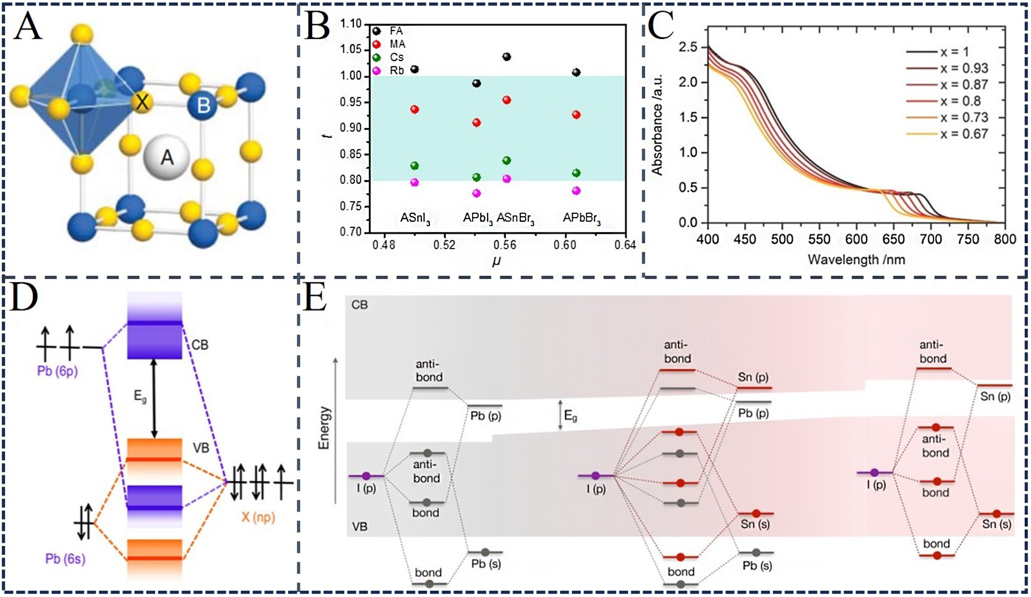
Figure 2. (A) 3D inorganic crystal structure with ABX3 formula; (B) The calculated t and μ factor values for halide perovskites; (C) Optical absorption spectra of CsPbIxBr3-x at different iodine concentrations. This figure is quoted with permission from Ref.[54], Copyright © 2016 Wiley-VCH; (D) The schematic diagram of bonding and antibonding orbitals in APbX3 illustrates the formation of the valence band and conduction band. This figure is quoted with permission from Ref.[57], Copyright © 2016 American Chemical Society; (E) Schematic diagram of bandgap bowing effect in CsPb1-xSnxI3. The shaded area represents the valence band and conduction band, while the thick lines illustrate the molecular orbital picture of the electronic energy bands in the Sn-Pb alloy. This figure is quoted with permission from Ref.[60], Copyright © 2018 American Chemical Society.

