

fig10
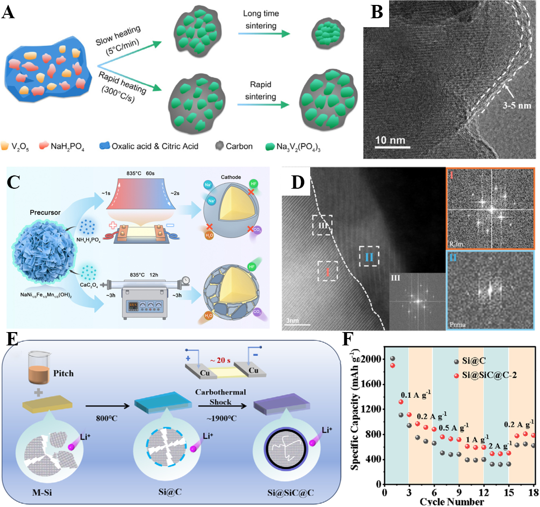
Figure 10. (A) Schematic diagram for synthesizing NVP@C[116]; (B) TEM image of NVP@C[116]; (C) Schematic diagram for preparing NFM333@NCP[117]; (D) High-angle annular dark field scanning transmission electron microscopy of NFM333@NCP[117]; (E) Schematic illustration for synthesizing Si@SiC@C[118]; (F) Rate performance of samples[118]. NVP@C: Na3V2(PO4)3@C; TEM: transmission electron microscope; NFM333@NCP: NaNi1/3Fe1/3Mn1/3O3@NaCaPO4.

