


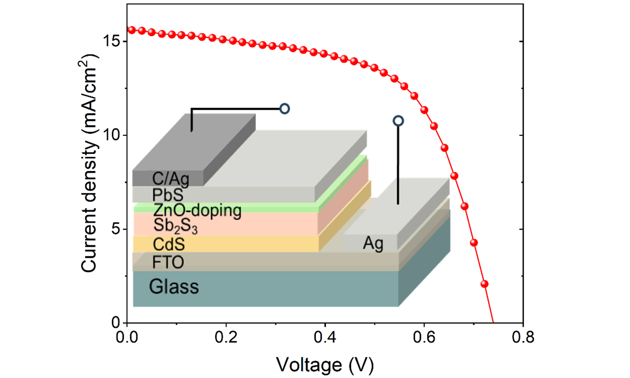
Zn doping modulation of carrier transport properties at the back interface of antimony sulfide solar cells
 0
0  ,
, Abstract
Sb2S3 has emerged as a highly promising material for thin-film solar cells due to its low toxicity, excellent stability, and strong light absorption in the visible region. However, challenges such as the formation of the Sb2O3 secondary phase and S re-evaporation still exist during the high-temperature annealing of Sb2S3. To address these issues, this study introduces a strategy involving the pre-deposition of an ultrathin ZnO protective layer onto the Sb2S3 surface. The ZnO layer facilitates controlled oxygen passivation through a lattice-vacancy-mediated mass transfer mechanism, effectively suppressing the formation of Sb2O3 and minimizing Sb2S3 volatilization, while simultaneously forming a Zn-doping layer. The results show that Zn doping significantly enhances the energy level alignment at the back interface: the conduction band minimum (CBM) and valence band maximum (VBM) of the Sb2O3/Sb2S3 mixed layer are upshifted, and the Fermi level is downshifted, thereby promoting hole transport. Additionally, the carrier concentration increases, reducing the contact barrier with the carbon electrode. This modification enables the power conversion efficiency (PCE) of all-inorganic Sb2S3 solar cells with fluorine-doped tin oxide (FTO)/CdS/Sb2S3/PbS/Carbon/Ag structures to reach an impressive 7.00%, representing the most advanced performance level currently available and providing new guidance for the development of high-performance and low-cost all-inorganic Sb2S3 solar cells.
Keywords
INTRODUCTION
In recent years, antimony-based solar cells have achieved rapid development due to their environmentally friendly characteristics and excellent physical properties[1,2]. Among them, antimony sulfide (Sb2S3) has gained significant attention as a promising light-absorbing material for thin-film solar cells, thanks to its near-ideal bandgap of 1.7 eV, high visible-light absorption coefficient (> 5 × 104 cm-1), low toxicity, and excellent environmental stability[3,4]. Since Savadogo’s pioneering work on chemically deposited Sb2S3 films and photoelectrochemical cells in 1992[5], substantial progress has been made[6,7]. Solution-based techniques, particularly chemical bath deposition (CBD) and hydrothermal synthesis, have dominated due to their low equipment requirements and scalability. Notably, in 2025, Shen et al. achieved a record-breaking 8.26% power conversion efficiency (PCE) by developing ethylenediaminetetraacetic acid disodium salt as an additive to regulate the reaction kinetics for Sb2S3 deposition[8]. However, these efficiencies remain significantly below the Shockley-Queisser (S-Q) limit (28.6%)[9]. The S-Q analysis predicts maximum values of open-circuit voltage (Voc) = 1.402 V, short circuit current density (Jsc) =
Annealing, as a crucial step after the deposition of Sb2S3 thin films, should be carried out at 300-450 °C, which drives the transformation of the amorphous phase to the crystalline phase through thermal rearrangement and simultaneously enhances the ion diffusion rate[10]. However, this process faces multiple challenges: Firstly, the essential annealing at high temperatures, aggravating the re-evaporation of sulfur and Sb2S3 due to their high saturated vapor pressure, leads to surface defects, film non-uniformity, and even exposure of the underlying CdS layer, which finally disrupts the integrity of the p-n junction. Secondly, residual oxygen reacting with antimony forms harmful Sb2O3 secondary phases at high temperature, which not only disrupts interface flatness and continuity but also introduces carrier recombination centers, significantly reducing device efficiency[11]. Thirdly, the re-crystallization of Sb2S3 delivers a low-level position of valence band energy which creates severe band mismatch with the back electrode. To address the above challenges, researchers have explored the introduction of stable metal oxide buffer layers at the back interface during annealing. For instance, a Ni/Ti co-doped MoO2 hole transport layer (HTL) can effectively extract holes from the metal halide perovskite layer, achieving a PCE of 18.1% in perovskite solar cells[12]. When WO3-x is used as the HTL, the formation of Sb-W bonds at the Sb2Se3/WO3-x interface creates an interface dipole, which not only reduces the hole extraction barrier but also effectively suppresses back interface recombination in Sb2Se3 devices[13]. Additionally, first-principles calculations by Professor Chen's team demonstrated that Zn doping in Sb2S3 can lower the Fermi level and increase the conductivity[14,15]. And Tang et al. further confirmed that solution-processed Zn doping can elevate the back surface energy level of Sb2S3, improve carrier transport, and reduce interface recombination[16]. These strategies based on oxide buffer layers or metal element doping all provide effective ways to improve the photovoltaic performance of Sb2S3.
Building on interface engineering and doping strategies, this work employs an ultrathin ZnO layer as an oxygen diffusion barrier, referred to as a “breathing membrane”. This layer enables controlled oxygen passivation of the underlying Sb2S3 film via a lattice-vacancy-mediated mass transfer mechanism, effectively inhibiting the formation of Sb2O3 and reducing interface defects, etc. Critically, the selection of ZnO also considers potential Zn2+ substitutional doping at the Sb2S3/oxide interface, which modulates interfacial energy levels and enhances carrier concentration. This synergistic approach concurrently optimizes the phase composition, morphology, and electrical properties of the Sb2S3 back surface, thereby improving
EXPERIMENTAL
Chemicals
Cadmium nitrate tetrahydrate [Cd(NO3)2·4H2O], ammonium hydroxide (NH3·H2O), thiourea (CH4N2S), and cadmium chloride hemipentahydrate (CdCl2·2.5H2O) were purchased from Sinopharm Chemical Reagent Co., Ltd. (Shanghai, China). Methanol (CH3OH), potassium antimony tartrate hemihydrate (C4H4KO7Sb·0.5H2O), and lead acetate trihydrate (PbC4H6O4·3H2O) were supplied by Shanghai Macklin Biochemical Co., Ltd. (Shanghai, China). Zinc oxide (ZnO), and sodium thiosulfate pentahydrate (Na2S2O3·5H2O) were supplied by Aladdin Reagent Co., Ltd. (Shanghai, China). The carbon ink (C, CH-8) was supplied by Jujo printing supplies & Technology Co. Ltd. (Zhejiang, China). The silver conductive paint (Ag, 05002-AB) was supplied by Structure Probe, Inc (USA). All the chemicals were used as received without further purification.
CdS electron transport layer preparation
Commercial FTO was ultrasonically cleaned with detergent, acetone, anhydrous ethanol, and ultrapure water sequentially for 60 min, dried, and ozone-treated for 20 min to remove surface organics/impurities. The FTO substrate with the conductive surface facing down was placed into a 100 mL deionized water solution containing 0.15 mM cadmium nitrate tetrahydrate, 9.4 mM thiourea and 0.19 mol ammonium hydroxide. The mixed solution was then placed in a 65 °C water bath for 15 min to deposit the CdS film. To improve the crystallinity, 0.05 g CdCl2·2.5H2O dissolved in 10 mL methanol was spin-coated on CdS, annealed in air at 380 °C for 5 min, then cooled naturally.
Sb2S3 and ZnO preparation
Dissolve 0.12 mol of sodium thiosulfate pentahydrate as the sulfur source and 0.06 mol of potassium antimony tartrate hemihydrate as the antimony source in 40 mL of deionized water respectively, then mix them to form 80 mL of solution. The mixture and three FTO/CdS substrates were transferred into a 100 mL Teflon-lined autoclave vessel. Seal the autoclave and heat it at 120 °C for 12 h. After the hydrothermal reaction, wash the sample with deionized water and then dry it under normal pressure on a hot plate to obtain the Sb2S3 precursor film.
Prepare the ZnO protective layer by radio frequency magnetron sputtering. The specific process parameters are as follows: the sputtering base pressure is less than 1.0 × 10⁻³ Pa, the working gas is a mixture of argon and oxygen (Ar:O2 = 9:1), the sputtering power is set at 60 W, and the sputtering time is controlled at 20-400 s. Then, place the sample in a closed space and perform annealing in an ambient air atmosphere in an inverted manner. The annealing temperature is 450 °C for 3 min. Nine devices were fabricated under each experimental condition to support statistical analysis.
HTL and Electrode fabrication
Deposit PbS by in-situ hydrothermal method. Dissolve 3.3 mM of lead acetate trihydrate (PbC4H6O4·3H2O) and 17.4 mM of sodium thiosulfate pentahydrate (Na2S2O3·5H2O) in 50 mL of deionized water to form a clear solution. Immerse the Sb2S3 film in the above solution in a 100 mL Teflon-lined autoclave, seal it, and heat it at 120 °C for 35 min. Apply carbon ink on the HTL and bake it at 120 °C on a hot plate for 30 min. Apply silver paste on the carbon layer and bake it at 80 °C for 10 min to complete the device fabrication. The total fabrication time for a complete device is approximately 2 to 3 days. Finally, a total of 54 devices were fabricated to validate the statistical reliability of the results.
Characterization
In this work, we used a field emission scanning electron microscope (SU-8010; Hitachi High-Tech, Japan) equipped with energy dispersive X-ray (EDX) to characterize the surface and elemental composition of the selenated antimony original mineral films. The crystal structures of the surface and powder of the selenated antimony original mineral films were characterized by X-ray diffraction (Ultima IV; Rigaku Corporation, Japan). The transmittance of the thin film was measured by ultraviolet–visible spectroscopy (UV-Vis) absorption spectroscopy (Lambda 950; PerkinElmer, USA). The current density-voltage (J-V) curves were collected using a Keithley 2400 source meter (Keithley 2400; Keithley Instruments, USA) under simulated AM 1.5G by the solar simulator (Newport 94023A; Newport Corporation, USA). The external quantum efficiency (EQE) of the devices was performed by a solar cell quantum efficiency measurement system (QEX10; PV Measurements, Inc., USA). Carrier transport and recombination mechanisms were investigated through electrochemical impedance spectroscopy (EIS) and dark capacitance-voltage (C-V) analysis. The Raman measurement was performed using the LABRAM-HR microRaman system with a 532 nm laser light source (LabRAM HR Evolution; HORIBA Scientific, France).
RESULTS AND DISCUSSION
The surface morphology of Sb2S3 precursor films, with and without the ZnO modification layer, was first analyzed by scanning electron microscopy (SEM). As depicted in Supplementary Figure 1, the deposition of an ultrathin ZnO layer did not significantly alter the initial morphology; both samples displayed characteristic large-grained structures formed from agglomerated nanocrystals, typical of hydrothermally grown Sb2S3 films. However, post-annealing morphological evolution revealed stark contrasts, as shown in Figure 1. The unmodified sample (W/O ZnO) formed ~50 nm Sb2O3/Sb2S3 particles and ~40 nm Sb2O3 nanobelts at grain boundaries. By contrast, ZnO-coated films exhibited notable morphological refinements: the 20 s ZnO sample showed smaller particles (~30 nm) and narrower nanobelts (~20 nm), with coarsening observed at longer deposition times. This coarsening is attributed to ZnO-mediated suppression of Sb2S3 volatilization, which increases the local Sb2S3 availability for oxidation and promotes Sb2O3 growth supported by subsequent compositional analysis.
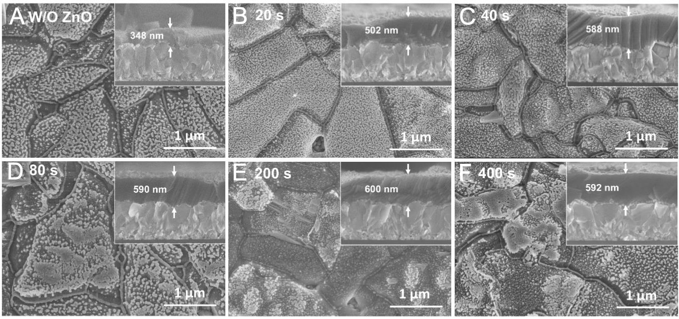
Figure 1. Surface and cross-sectional morphologies of Sb2S3 thin films (A) without ZnO and with ZnO deposited with (B) 20 s, (C) 40 s, (D) 80 s, (E) 200 s and (F) 400 s. SEM: Scanning electron microscope; W/O: without ZnO.
Cross-sectional SEM imaging (the inset of Figure 1) corroborated these findings. The control film (W/O ZnO) displayed a highly uneven thickness (~350 nm) due to extensive Sb2S3 loss during annealing, along with the presence of large Sb2O3 surface particles. Incorporation of a 20 s ZnO layer mitigated volatilization, resulting in a more uniform film with increased thickness (~500 nm). Extended ZnO deposition (≥ 40 s) further improved thickness (up to ~600 nm) and significantly reduced Sb2O3 surface features. Elemental analysis via energy-dispersive X-ray spectroscopy (EDS) quantified atomic percentages of Sb, S, O, and Zn [Supplementary Figure 2A]. Key trends include: (1) relatively stable Sb content, (2) a non-monotonic variation in S content, (3) an initial decrease followed by an increase in O content, and (4) a clear upward trend in Zn concentration (from ~0.1% to ~1.2 at.%). The elevated oxygen and decreased sulfur levels at
To evaluate the photovoltaic impact of ZnO incorporation, Sb2S3 solar cells were fabricated using a hydrothermally deposited PbS HTL, paste-coated carbon and Ag contacts. The statistical results of the average values of J-V measurements [Figure 2A and Table 1] show that the enhancement effect of the ZnO modified devices is consistent. The Voc remained above 700 mV for all ZnO-treated samples, peaking at 40 s due to reduced Sb2S3 degradation and minimized leakage pathways. The optimal 40 s ZnO condition coincides with minimized resistive Sb2O3 formation and improved bulk conductivity, facilitating efficient carrier extraction. The Jsc increased by 17% at 40 s ZnO (14.6 mA/cm2) compared to the control, then declined with thicker ZnO layers. Similarly, the FF reached an optimal average of 59% at 40 s, but dropped to ~50% at ≥ 80 s, consistent with increased series resistance and impeded hole transport from thicker ZnO layers. Consequently, the highest PCE of 7.00% was attained under 40 s ZnO conditions (Voc = 729 mV, Jsc = 15.6 mA/cm2, FF = 61.5%), representing a 20% improvement over the unmodified reference device. Although this device performance still lags behind that of Spiro-OMeTAD/metal electrodes and Sb2S3-based tandem devices[17,18], this study provides a practical strategy for the low-cost fabrication of solar cells employing all-inorganic carbon electrodes.
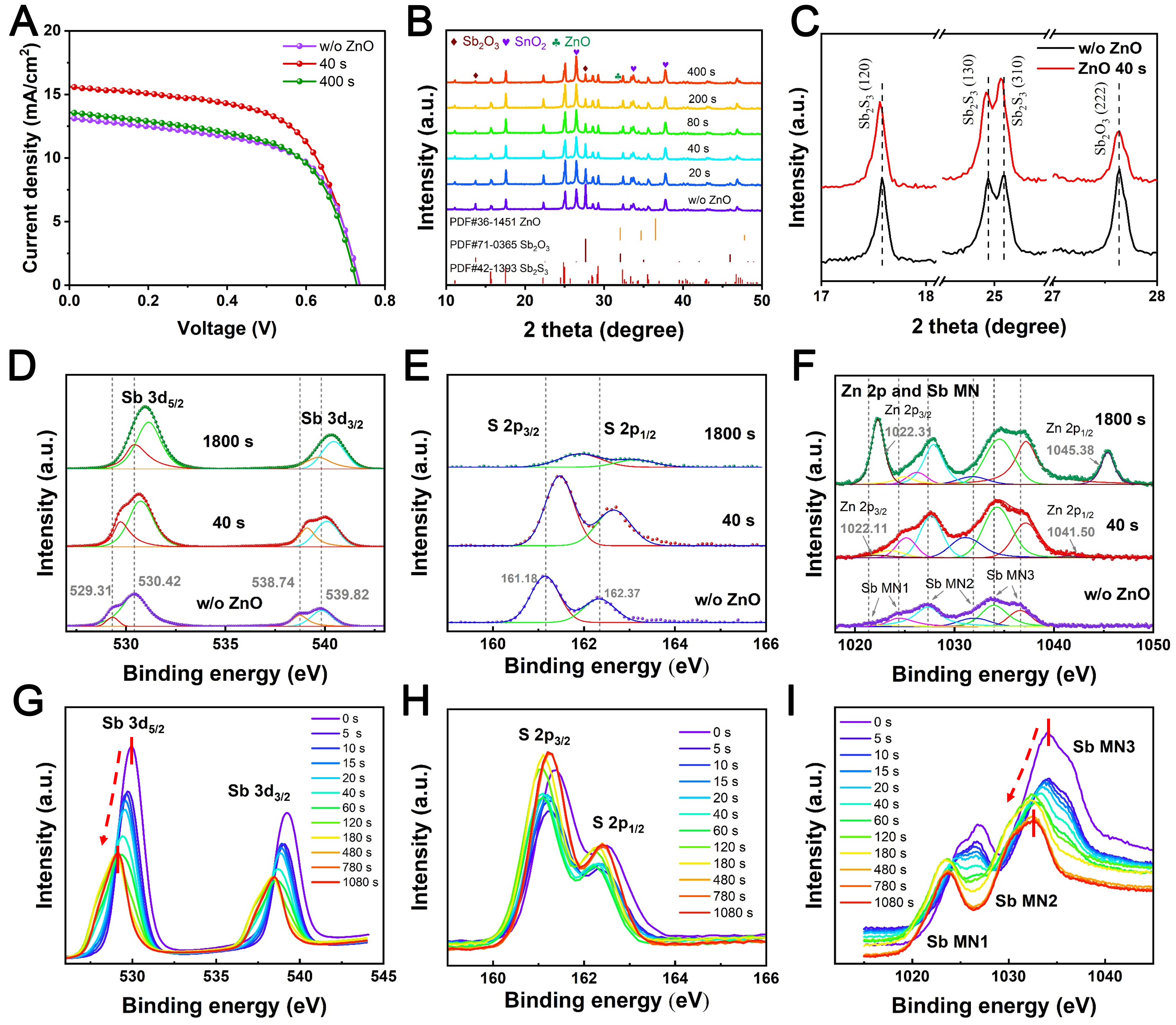
Figure 2. (A) J-V curves and (B) XRD patterns of Sb2S3 doped with ZnO with different deposition times; (C) The magnified XRD pattern of the Sb2S3 films; (D) Sb 3d, (E) S 2p and (F) Zn 2p XPS spectra of Sb2S3 thin films with and without ZnO. High-resolution (G) Sb 3d, (H)
The performance parameters list of Sb2S3 solar cells without and with ZnO
| Sample | Voc (mV) | Jsc (mA/cm2) | Rs (Ω) | Rsh (kΩ) | FF (%) | PCE (%) |
| W/O ZnO | 729 6 | 12.5 1.2 | 158 86 | 3.2 0.4 | 56 6 | 5.1 0.9 |
| 20 s | 727 8 | 13.4 0.7 | 143 49 | 3.0 0.2 | 58 4 | 5.4 0.6 |
| 40 s | 728 9 | 14.6 0.6 | 111 11 | 3.2 0.2 | 59 1 | 6.6 0.3 |
| 80 s | 716 14 | 13.3 1.2 | 182 51 | 2.3 0.7 | 50 5 | 4.4 0.7 |
| 200 s | 715 15 | 12.0 0.9 | 238 106 | 2.1 0.5 | 46 5 | 4.0 0.5 |
| 400 s | 725 10 | 12.1 0.8 | 333 79 | 2.6 0.7 | 43 5 | 3.7 0.6 |
X-ray diffraction (XRD) analysis [Figure 2B] verified the crystallographic composition of annealed films, identifying orthorhombic Sb2S3 (PDF#42-1393) as the dominant phase, with minor peaks corresponding to cubic Sb2O3 (PDF#71-0365). Notably, the intensity of the Sb2O3 (222) peak at 27.68° decreased systematically with longer ZnO deposition [Supplementary Figure 3A and B], indicating suppressed secondary oxide formation. A weak ZnO (100) peak appeared only at 80 s ZnO, while no ZnO diffraction was detectable at shorter deposition times (≤ 40 s), underscoring the ultrathin and amorphous nature of ZnO in those cases. These results confirm that the ZnO interlayer effectively retards Sb2O3 phase formation during air annealing.
To understand the origin of these enhancements, grazing-incidence XRD (GIXRD) at 2o incidence [Supplementary Figure 4] revealed no residual ZnO phase in the 40 s ZnO film post-annealing, suggesting Zn substitution within the Sb2S3 or Sb2O3 lattices. Detailed peak analysis [Figure 2C] showed systematic shifts of major Sb2S3 and Sb2O3 peaks toward higher angles, consistent with lattice contraction per Bragg’s law
X-ray photoelectron spectroscopy (XPS) was employed to elucidate the Zn chemical state. Survey scans [Supplementary Figure 5] confirmed elemental presence of C, Sb, S, O, and Zn. High-resolution Sb 3d spectra [Figure 2D] revealed that ZnO deposition reduced Sb2O3 content from 79% (control) to 65% (40 s ZnO), consistent with SEM/XRD trends. The S 2p spectrum [Figure 2E] showed typical spin-orbit splitting indicative of S2- in Sb2S3, with a shift to higher binding energies upon ZnO deposition, suggesting reduced sulfur vacancies. Zn 2p peaks [Figure 2F] were absent in the control but faintly detected at 1,022.11 eV and 1,045.50 eV in the 40 s ZnO sample. This chemically shift relative to crystalline ZnO indicates incorporation rather than phase separation. Concurrent shifts in Sb MNN Auger peaks further suggest Zn-S bonding and altered Sb electronic environments.
To probe the depth distribution of Zn doping, XPS depth profiling was performed on the Zn-doping sample (40 s ZnO) versus the control (W/O ZnO) using Ar+ sputtering at 0.03 nm/s. The Sb 3d5/2 binding energy [Figure 2G] decreased with sputtering time, stabilizing beyond 200 s (~6 nm depth). Quantifying the Sb 3d5/2 shift relative to the unsputtered surface (Supplementary Figure 6, red spheres) showed an exponential decay (y = -0.91 + 0.73e-x/60), with stabilization beyond 200 s (~6 nm depth). This confirms a thin Sb2O3 surface layer serving as a hole-blocking but tunnel-permissive oxide. This structure is beneficial for suppressing interfacial recombination while enabling charge extraction. Concurrently, smaller S 2p shifts [Figure 2H and Supplementary Figure 6] and analogous Sb MNN Auger peak displacements (Figure 2I, Supplementary Figure 6, fit: y = -1.52 + 1.72e-x/42) indicate ZnSb substitutional doping confined primarily to the top ~10 nm. ZnSb substitution was confined to the top ~10 nm, supported by S 2p and Sb MNN trends [Figures 2H and I, Supplementary Figure 6]. This confirms that the ZnO cap limits Sb2O3 formation to an ultrathin ~6 nm layer, functioning as a wide-bandgap hole-blocking layer. Then it suppresses interfacial recombination while enabling efficient hole tunneling due to its minimal thickness, consistent with enhanced Jsc. Collectively, these depth-resolved analyses demonstrate the dual role of the ZnO interlayer: (1) restricting Sb2O3 to nanoscale surface regions, and (2) enabling shallow Zn doping in Sb2S3.
To correlate these interfacial modifications with carrier dynamics, light-intensity-dependent Jsc and Voc measurements were conducted [Figure 3]. According to the power-law relationship [Equation 1][19], the fitting can obtain the α value.
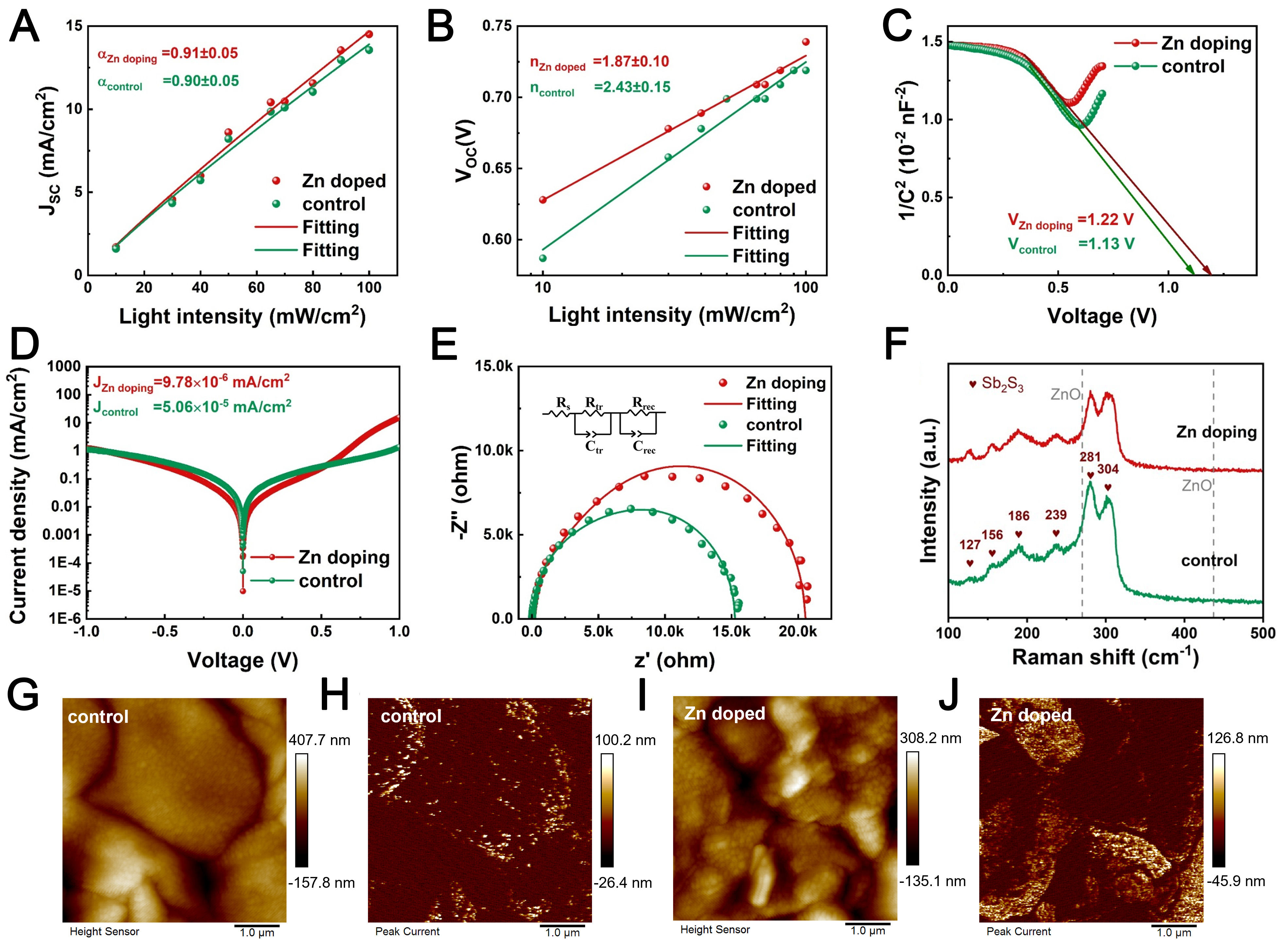
Figure 3. (A) Jsc, (B) Voc as a function of light intensity (C) 1/C2-V curves of Sb2S3 devices; (D) Dark J-V curves and (E) Nyquist plots of Sb2S3 devices; (F) Raman spectra of control and Zn doping Sb2S3 thin films; (G and H) AFM images and (I and J) C-AFM images of control and Zn doping Sb2S3 thin films. J-V: Density-voltage; Voc: open-circuit voltage; C-AFM: conductive atomic force microscopy; Rtr: charge transport resistance; Rrec: recombination resistance; Jsc: short-circuit current density; Rs: series resistance; Ctr and Crec: capacitor.
Where I represents the percentage of irradiation light intensity, and α is the power exponent. As shown in the Jsc and irradiation light intensity relationship graph in Figure 3A, yielded α = 0.90 (control) versus 0.91 (Zn-doping), indicating marginally improved carrier collection efficiency. More significantly, the function relationship between Voc and light intensity satisfies[20]:
where T, kB (1.38 × 10⁻²³ J/K), and q (1.60 × 10⁻¹⁹ C) are the Kelvin temperature, Boltzmann constant, and elementary charge, respectively, and n is the ideality factor related to recombination. The diode ideality factor n extracted from decreased from 2.43 (control) to 1.87 (Zn-doping), demonstrating substantial suppression of Shockley-Read-Hall (SRH) recombination via Zn-induced defect passivation. These carrier transport enhancements directly explain the observed performance gains.
The C-V characteristics of photovoltaic devices under dark conditions provide critical insights into defect-related properties. We thus measured dark C-V curves at 2 kHz with a 30 mV alternating current (AC) amplitude
Here, C is the capacitance, V is the applied DC bias, S (0.09 cm2) is the cell area, ε0 (8.854 × 10⁻¹⁴ F/cm) is the vacuum permittivity, and εp (6.67) is the relative permittivity of Sb2S3. The control device exhibited a lower Vbi (1.13 V) than the Zn-doping counterpart (1.22 V), aligning with the trend in Voc. The hole concentration (NA) of Sb2S3, derived from the slope of the linear fit, increased from 1.32 × 1016 cm-3 (control) to 1.47
Dark J-V characteristics further elucidate diode behavior [Figure 3D]. The reverse saturation current (J0) decreased significantly from 5.06 × 10⁻⁵ mA/cm2 (control) to 9.78 × 10⁻⁶ mA/cm2 (Zn-doping), indicating suppressed carrier recombination at the back interface. To gain further insight into the underlying carrier recombination and transport dynamics, we performed EIS measurements under dark conditions and acquired the corresponding Nyquist plots (Figure 3E, inset showing the equivalent circuit). Among them, the charge transport resistance (Rtr) characterizes the carrier collection capability, while the recombination resistance (Rrec) is inversely proportional to the carrier recombination rate of the device. Fitted parameters [Supplementary Table 1] revealed that reduced charge transport resistance (Rtr = 3.2 kΩ target vs. 5.2 kΩ control) confirms enhanced carrier collection, and increased recombination resistance (Rrec = 17 kΩ target vs. 10 kΩ control), which inversely correlates with recombination rates[21]. In summary, dark J-V and EIS analyses demonstrate that Zn doping concurrently suppresses carrier recombination and enhances transport/extraction efficiency, directly corroborating the observed performance improvements.
The foregoing analysis demonstrates that Zn doping at the Sb2S3 back surface enhances carrier concentration, suppresses recombination, and improves carrier transport efficiency, particularly boosting Jsc. To elucidate the underlying physical origins, we systematically investigated the chemical bonding, electronic properties, and energy-level alignments of Zn-doping Sb2S3 films. Raman spectroscopy [Figure 3F] revealed no ZnO characteristic peaks (dashed lines in Figure 3F) in either control or Zn-doping films. All observed peaks correspond exclusively to Sb2S3 vibrational modes[23]. The Raman spectrum of Sb2S3 arises from four vibrational modes (2A1 + 2E) of its tetrahedral SbS3 units (C3v symmetry): symmetric stretch νs (A1), asymmetric stretch νa (E), symmetric bend δs (A1), and asymmetric bend δa (E), with typical intensity ordering νs > νa and δs > δa[24]. As shown in Figure 3F, both films exhibit dominant peaks at 281 cm-1 [νa (Sb-S)] and 304 cm-1 [νs (Sb-S)], alongside weaker features at 127 cm-1 (Ag), 156 cm-1 (B1g), 189 cm-1 [δa > (S-Sb-S)], and 239 cm-1 [δs (S-Sb-S)]. Critically, the intensity ratio I304/I281 of symmetric-to-asymmetric stretching vibrations inversely correlates with sulfur vacancy (VS) concentration. Spectral deconvolution [Supplementary Figure 8A and B] yielded I304/I281 = 1.05 (control) versus 1.30 (Zn-doping), confirming reduced VS defects in the Zn-doping film. This reduction is attributed to suppressed Sb2S3 volatilization and enhanced crystallinity during ZnO-capped annealing, consistent with diminished non-radiative recombination observed in carrier dynamics.
To further probe the local electrical properties, conductive atomic force microscopy (C-AFM) was performed under dark conditions on both control and Zn-doping Sb2S3 films [Figure 3G-J]. Significantly elevated current signals were detected within the large-grained structures of the Zn-doping film compared to the reference. Concurrently, regions passivated by Sb2O3 nanobelts at grain boundaries exhibited further suppressed current leakage. These observations collectively demonstrate that enhanced bulk conductivity in Zn-doping Sb2S3 directly contributes to higher Jsc. While effective defect passivation at grain boundaries via oxygen incorporation, mitigating carrier recombination. These nanoscale electrical characteristics align consistently with the macroscopic device performance enhancements.
To elucidate carrier transport mechanisms, ultraviolet photoelectron spectroscopy (UPS) was performed on control and Zn-doping Sb2S3 films. The Fermi level (EF) and VBM positions were determined by subtracting the secondary electron cutoff edge from the He I excitation source (21.22 eV) [Figures 4A and B]. The control film exhibited EF = -3.48 eV and VBM = -6.04 eV, while Zn doping shifted these to EF = -3.70 eV and VBM = -5.99 eV. Given the mixed-phase surface composition (> 80% Sb2O3), the conduction band minimum (CBM) was referenced to Sb2O3’s bandgap. The proposed energy band diagram (Figure 4C, partial data adapted from Ref.[25]) reveals that the control device possesses high CBM and deep VBM at the back surface form an electron-blocking barrier, which suppresses recombination and transport holes through the oxide tunnel. For Zn-doping device, a 0.22 eV downward shift in EF and 0.05 eV upward shift in VBM/CBM collectively enhance back-surface field strength. Coupled with the ultrathin oxide layer (< 10 nm), this configuration promotes hole separation, directly explaining the enhanced Voc and Jsc and PCE.
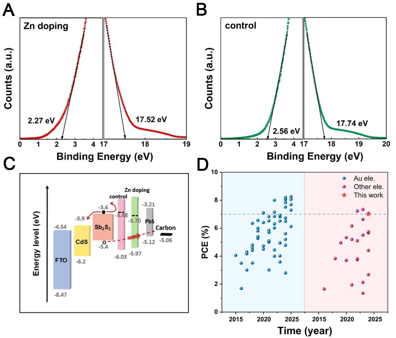
Figure 4. UPS spectrum of (A) control and (B) Zn doping Sb2S3 thin films; (C) schematic band diagram and (D) the summarized PCE of previous works of Sb2S3 solar cell. UPS: Ultraviolet photoelectron spectroscopy; FTO: fluorine-doped tin oxide; CdS: cadmium sulfide; PCE: power conversion efficiency.
The successful incorporation of Zn and the concomitant suppression of Sb2O3 underscore the dual functionality of our ultrathin ZnO layer strategy. This feature distinguishes it from conventional single-function strategies. For instance, prior approaches to alleviate back-contact issues often relied on introducing distinct metal oxide buffer layers (e.g., WO3-x, MoO2) primarily for hole transport or energy level alignment[13,17], or focused solely on elemental doping (e.g., solution-processed Zn doping) to tailor electrical properties[16]. While effective, these strategies typically address only one aspect of the complex interfacial challenges in Sb2S3-based devices. Our approach uniquely integrates a diffusion barrier and a dopant source into a single sub-nanometer-scale layer, simultaneously tackling phase purity, defect passivation, and energy level modulation. This synergistic effect is evidenced by the concurrent improvement in NA, Rrec, and Voc.
Through the strategic implementation of a ZnO protective layer, we optimized both the Sb2O3 thickness and achieved surface Zn-doping in Sb2S3, culminating in a 7.00%-efficient, fully inorganic carbon-electrode-based Sb2S3 solar cell with an FTO/CdS/Sb2S3/PbS/Carbon/Ag architecture. Statistically compiled literature data [Figure 4D] position this efficiency at the state-of-the-art performance tier for planar Sb2S3 thin-film devices {Surpassing the 7% benchmark indicated by the gray dashed line, and the references are presented in Supplementary Materials [1-90]}. Notably, previously reported high-efficiency Sb2S3 devices predominantly employ unstable organic hole-transport layers (e.g., Spiro-OMeTAD or P3HT) and cost-prohibitive Au electrodes, fundamentally limiting their practical viability. In contrast, our approach leverages ambient air-annealing and low-cost carbon electrodes to construct an all-inorganic device, which exhibits the competitive efficiency approaching the current Sb2S3 record. Based on the enhanced operational stability from inorganic constituents and scalable manufacturability via solution-processable components[26], this work establishes a transformative pathway toward economically viable, high-performance thin-film solar cells.
CONCLUSION
In this work, we aimed to address the critical challenges of sulfur volatilization and detrimental Sb2O3 formation at the back interface of Sb2S3 solar cells during high-temperature annealing. By introducing an ultrathin ZnO protective layer, we developed a dual-functional strategy that simultaneously achieves controlled oxygen passivation and effective Zn doping. This synergistic modification suppresses interfacial recombination, optimizes energy level alignment, and enhances carrier transport. Ultimately, in comparison with unmodified devices, the ZnO-modified solar cells exhibit a 17% enhancement in Jsc and a significant improvement in PCE, culminating in a state-of-the-art PCE of 7.00% for fully inorganic, carbon-based architectures. This scalable and air-processable strategy provides a promising route toward high-performance, stable, and low-cost Sb2S3 solar cells.
DECLARATIONS
Authors’ contributions
Idea conception: Chen, G. L.
Writing - original draft: Xia, Y. S.
Writing - editing: Chen, S.; Huang, Z. P.; Li, H.; Lin, L. M.; Xia, Y. S.
Materials characterization: Zhang, J. C.; Cai, J. R.; Huang, G.; Xia, Y. S.
Samples synthesis: Huang, J.; Liu, L. J.; Chen, S.; Xia, Y. S.
Funding acquisition, supervision: Chen, G. L.
All authors participated in the data analysis and result discussions and commented on the manuscript.
Availability of data and materials
The data that support the findings of this study are available from the corresponding author upon reasonable request.
AI and AI-assisted tools statement
Not applicable.
Financial support and sponsorship
This work was supported by the National Natural Science Foundation of China (Grant Nos. 62475044; 62204041), Natural Science Foundation of Fujian Province (Grant Nos. 2025J010031; 2025H6009; 2023I0012).
Conflicts of interest
All authors declared that there are no conflicts of interest.
Ethical approval and consent to participate
Not applicable.
Consent for publication
Not applicable.
Copyright
© The Author(s) 2026.
Supplementary Materials
REFERENCES
1. Zheng, J.; Liu, C.; Zhang, L.; et al. Enhanced hydrothermal heterogeneous deposition with surfactant additives for efficient Sb2S3 solar cells. Chem. Eng. J. 2022, 446, 136474.
2. Liu, C.; Gong, A.; Zuo, C.; et al. Heterojunction lithiation engineering and diffusion-induced defect passivation for highly efficient Sb2(S,Se)3 solar cells. Energy. Environ. Sci. 2024, 17, 8402-12.
3. Ghosh, C.; Varma, B. Optical properties of amorphous and crystalline Sb2S3 thin films. Thin. Solid. Films. 1979, 60, 61-5.
5. Zhao, R.; Yang, X.; Shi, H.; Du, M. Intrinsic and complex defect engineering of quasi-one-dimensional ribbonsSb2S3 for photovoltaics performance. Phys. Rev. Mater. 2021, 5, 054605.
6. Wang, S.; Zhao, Y.; Che, B.; et al. A novel multi-sulfur source collaborative chemical bath deposition technology enables 8%-efficiency Sb2S3 planar solar cells. Adv. Mater. 2022, 34, 2206242.
7. Li, Y.; Li, R.; Jia, Z.; et al. Precursor engineering of solution-processed Sb2S3 solar cells. Small 2024, 20, 2308895.
8. Shen, G.; Ke, A.; Chen, S.; et al. Strong chelating additive and modified electron transport layer for 8.26%‐efficient Sb2S3 solar Cells. Adv. Energy. Mater. 2025, 15, 2406051.
9. Shockley, W.; Queisser, H. J. Detailed balance limit of efficiency of p-n junction solar cells. J. Appl. Phys. 1961, 32, 510-9.
10. Yao, L.; Lin, L.; Huang, Z.; et al. A liquid medium annealing strategy for highly [041]/[141]-oriented planar antimony sulfide solar cells with 7.23% efficiency. Nano. Energy. 2023, 106, 108064.
11. Chen, C.; Zhao, Y.; Lu, S.; et al. Accelerated optimization of TiO2/Sb2Se3 thin film solar cells by high‐throughput combinatorial approach. Adv. Energy. Mater. 2017, 7, 1700866.
12. Heo, J. H.; Im, K.; Lee, H. J.; Kim, J.; Im, S. H. Ni,Ti-co-doped MoO2 nanoparticles with high stability and improved conductivity for hole transporting material in planar metal halide perovskite solar cells. J. Ind. Eng. Chem. 2021, 94, 376-83.
13. Liu, C.; Shen, K.; Lin, D.; et al. Back contact interfacial modification in highly-efficient all-inorganic planar n-i-p Sb2Se3 Solar Cells. ACS. Appl. Mater. Interfaces. 2020, 12, 38397-405.
14. Cai, Z.; Dai, C.; Chen, S. Intrinsic defect limit to the electrical conductivity and a two‐step p‐type doping strategy for overcoming the efficiency bottleneck of Sb2S3‐based solar cells. Solar. RRL. 2019, 4, 1900503.
15. Cai, Z.; Chen, S. Extrinsic dopants in quasi-one-dimensional photovoltaic semiconductor Sb2S3: a first-principles study. J. Appl. Phys. 2020, 127, 183101.
16. Tang, R.; Wang, X.; Jiang, C.; et al. n-type doping of Sb2S3 light-harvesting films enabling high-efficiency planar heterojunction solar cells. ACS. Appl. Mater. Interfaces. 2018, 10, 30314-21.
17. Chen, S.; Li, M.; Zhu, Y.; et al. A codoping strategy for efficient planar heterojunction Sb2S3 solar cells. Adv. Energy. Mater. 2022, 12, 2202897.
18. Chen, S.; Zhao, X.; Shen, G.; et al. All-inorganic Sb2S3-based two-terminal tandem solar cells enable over 10.9% efficiency employing a concise interconnection layer. J. Mater. Chem. A. 2024, 12, 18148-56.
19. Wang, X.; Tang, R.; Jiang, C.; et al. Manipulating the electrical properties of Sb2(S,Se)3 film for high‐efficiency solar cell. Adv. Energy. Mater. 2020, 10, 2002341.
20. Jiang, C.; Zhou, J.; Tang, R.; et al. 9.7%-efficient Sb2(S,Se)3 solar cells with a dithieno [3,2-b: 2’,3’-d] pyrrole-cored hole transporting material. Energy. Environ. Sci. 2021, 14, 359-64.
21. Yin, Y.; Wu, C.; Tang, R.; et al. Composition engineering of Sb2S3 film enabling high performance solar cells. Sci. Bull. 2019, 64, 136-41.
22. Heath, J. T.; Cohen, J. D.; Shafarman, W. N. Bulk and metastable defects in CuIn1-xGaxSe2 thin films using drive-level capacitance profiling. J. Appl. Phys. 2004, 95, 1000-10.
23. Lin, L.; Liu, J.; Lv, J.; et al. Correlation between native defects and morphological, structural and optical properties of ZnO nanostructures. J. Alloys. Compd. 2017, 695, 1523-7.
24. Hajdeu-Chicarosh, E.; Rotaru, V.; Levcenko, S.; et al. Raman scattering and spectroscopic ellipsometry studies of Sb2S3 and Sb2Se3 bulk polycrystals. Phys. Chem. Chem. Phys. 2023, 25, 31188-93.
25. Wu, F.; Zhao, Y.; Yao, L.; et al. Manipulating back contact enables over 8%-efficient carbon-based Sb2(S,Se)3 solar cells. Chem. Eng. J. 2022, 440, 135872.
Cite This Article
How to Cite
Download Citation
Export Citation File:
Type of Import
Tips on Downloading Citation
Citation Manager File Format
Type of Import
Direct Import: When the Direct Import option is selected (the default state), a dialogue box will give you the option to Save or Open the downloaded citation data. Choosing Open will either launch your citation manager or give you a choice of applications with which to use the metadata. The Save option saves the file locally for later use.
Indirect Import: When the Indirect Import option is selected, the metadata is displayed and may be copied and pasted as needed.
About This Article
Special Topic
Copyright

Data & Comments
Data
0


Comments
Comments must be written in English. Spam, offensive content, impersonation, and private information will not be permitted. If any comment is reported and identified as inappropriate content by OAE staff, the comment will be removed without notice. If you have any queries or need any help, please contact us at [email protected].