


Enhanced efficiency of Sb2S3 solar cells via heterojunction interfacial MgCl2-CdCl2 mixed treatment
 0
0 
Abstract
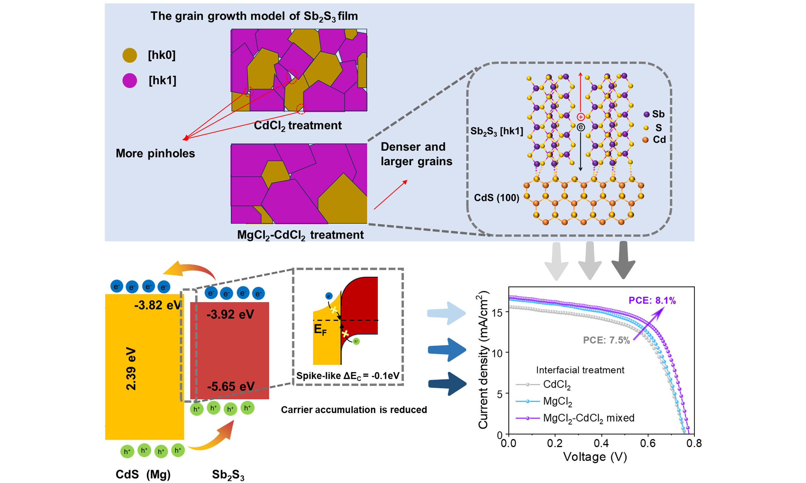
Antimony sulfide (Sb2S3) solar cells exhibit significant potential in tandem and indoor photovoltaic applications. The quality of cadmium sulfide (CdS)/Sb2S3 heterojunction, affected by energy-level misalignments and lattice-mismatch defects, is crucial for achieving high-performance devices. Herein, we propose a MgCl2-CdCl2 mixed treatment strategy for the CdS/Sb2S3 interface to suppress interfacial recombination caused by defects and energy band offsets. The obtained preferentially [100]-oriented CdS film effectively mitigates lattice mismatch and induces the subsequent hydrothermal deposition of a well-crystallized, vertically oriented Sb2S3 absorber. The MgCl2-CdCl2 mixed treatment introduces Mg2+ doping in the CdS layer, achieving an enhanced surface potential and well-matched interfacial energy band alignments. The CdS/Sb2S3 heterojunction interface forms a spike-type energy band structure with a small conduction band offset. Compared with the conventional CdCl2 treatment, the MgCl2-CdCl2 mixed-treated device exhibits a stronger built-in electric field (1.31 V) and low-temperature activation energy (1.63 eV), indicating the suppression of carrier recombination. Consequently, the champion Sb2S3 solar cells achieve an improved efficiency from 7.5% to 8.1%. This heterojunction treatment strategy is expected to provide an effective method for fabricating high-performance inorganic thin film solar cells.
Keywords
INTRODUCTION
Antimony sulfide (Sb2S3) solar cells have received widespread attention owing to their non-toxicity, low cost, and high stability. Sb2S3 films possess a relatively low melting point (~550 °C), enabling the production of highly crystalline films at relatively low temperatures and thereby reducing energy consumption during device fabrication[1]. Additionally, their bandgap (1.7 eV) is suitable for applications in Si-based top cells[2], indoor photovoltaics[3,4], photodetectors[5,6], and optical communication systems[7]. According to the Shockley-Queisser limit theory[8], the theoretical maximum power conversion efficiency (PCE) for a single-junction Sb2S3 solar cell can reach 28%. After over a decade of development, the highest PCE of Sb2S3 solar cells was reported to be 8.26%[9]. Despite this progress, the performances of Sb2S3 solar cells remain substantially lower than those of established technologies. The main issue is the large open-circuit voltage (VOC) loss caused by interfacial defects and recombination. The performance of the Sb2S3 solar cell can be significantly improved after addressing the limiting factors of the heterojunction interface.
Cadmium sulfide (CdS) with good photovoltaic properties is widely used as an electron transport layer (ETL) in Sb2S3 solar cells. However, the interfacial energy-level misalignment and lattice mismatch at the CdS/Sb2S3 heterojunction lead to severe interface recombination and carrier loss[10,11]. In addition, the high absorption of the CdS layer in the short-wavelength region (300-500 nm) reduces the light utilization efficiency of the Sb2S3 absorber layer[12]. Therefore, the CdS/Sb2S3 heterojunction quality is particularly important for the performance of the device. Currently, there are numerous heterojunction optimization strategies, such as ion doping, interface modification, energy level regulation, and post-processing[13-16]. Shen et al.[17] inserted an ultra-thin amorphous ETL at the heterojunction, which can improve interfacial carrier extraction. Liu et al.[18] developed a core/shell-structure interfacial layer in the Sb2S3 solar cell, boosting the photovoltaic performance. According to reports, cations (e.g., Al3+) can be doped into CdS to replace Cd2+, forming substitution defects[19] and increasing the N-type doping concentration. In addition, the monovalent cation Ag+ was doped in CdS, which enhances the conductivity of the CdS film anomalously and reduces its parasitic absorption simultaneously[20]. Interface post-processing is an effective approach to achieve interface optimization and suppress interfacial recombination effects. Most reported studies on halide-based treatments have focused on the absorber layer surface of Sb-based solar cells. Zhao et al. regulated an alkali metal fluoride post-treatment to fabricate high-performance Sb2(S,Se)3 solar cells by improving absorber crystallinity and conductivity[21]. Shen et al. developed a PbCl2 post-treatment onto the Sb2S3 back surface to passivate interfacial defects and reduce non-radiative recombination of the Sb2S3 solar cell, resulting in a significant increase in fill factor (FF)[22]. This indicates that halide-based strategies to treat the absorber layer help to enhance crystallization and improve orientation. For CdS treatment, SbCl3 treatment has been shown to improve the quality of CdS films and optimize energy band alignment at the CdS/Sb2Se3 interface[23]. At present, the CdCl2 treatment for CdS films is a widely used processing method. It can broaden the bandgap of CdS and reduce S vacancy defects in CdS[24]. Besides, the Cl doping of the absorber layer can passivate S vacancy defects[25], contributing to the suppression of VOC loss.
In this work, we propose a MgCl2-CdCl2 mixed heterojunction interface treatment strategy for Sb2S3 thin-film solar cells to suppress interfacial recombination and improve device efficiency. The introduction of Mg2+ into CdS film induces preferential growth of cubic-phase CdS along the (100) crystallographic plane, promoting vertical orientation growth in the absorber. Meanwhile, this mixed treatment optimizes the band alignment at the CdS/Sb2S3 heterojunction interface, effectively suppressing carrier accumulation at the interface. Systematic characterizations such as Kelvin probe force microscopy (KPFM) and variable-temperature measurement are used to demonstrate the physical mechanism of the photocarrier transport and recombination. The results show that the treatment enhances the built-in electric field and low-temperature activation energy (Ea), thereby overcoming VOC loss. The good crystallinity, interface defect passivation, and well-matched energy band alignments enable 8.1% efficiency of the Sb2S3 solar cells.
EXPERIMENTAL
Preparation of CdS film and treatment
CdS films were prepared on fluorine-doped tin oxide (FTO) substrates using the chemical bath method (CBD). First, FTO glass substrates were ultrasonically cleaned for 20 min each in detergent, anhydrous ethanol, acetone, and deionized water, followed by nitrogen drying. Next, 32 mL of 15 mM CdSO4 (99.99%, Macklin) and 40 mL of aqueous ammonia solution (25%-28%, Sinopharm) were sequentially added to 220 mL of deionized water, preheated at 66 °C for 2 min, and then 16 mL of 1.5 M thiourea (99.0%, Sinopharm) was added to the solution. The FTO substrate was vertically immersed in the precursor solution and maintained at 66 °C for 18 min to obtain a CdS layer approximately 60 nm thick. The MgCl2-CdCl2 mixed heterojunction interface treatment of CdS films was utilized by spin coating the MgCl2-CdCl2 mixed methanol solution at 4,000 revolutions per minute (rpm) for 20 s. Under fixing CdCl2 concentration of 15 mg/mL, the Mg/Cd molar ratios are controlled as 0.45, 0.9, and 1.35 by regulating MgCl2 concentration of 5, 10, and 15 mg/mL. The CdS samples were dried in air at 80 °C for 5 min to remove residual solvent and then annealed at 400 °C for 10 min.
Device fabrication
Sb2S3 films were prepared via a hydrothermal deposition method using C8H4K2O12Sb2·3H2O (99.9%, Aladdin, Shanghai, China) and Na2S2O3·5H2O (99.99%, Aladdin) as the source materials for antimony and sulfur, respectively. Specifically, 40 mL of 40 mM C8H4K2O12Sb2·3H2O solution was stirred for 3 min until the solution color changed from transparent to slightly yellow. The mixed solution was transferred to a 50 mL polytetrafluoroethylene (Teflon) reaction vessel, which was then sealed within a stainless-steel reaction vessel. The mixture was maintained at 130 °C for 180 min to obtain the Sb2S3 precursor film. The deposited film is then annealed in a rapid thermal annealing tube furnace (OTF-1200X, Kejing, Hefei, China) under an Ar atmosphere at 370 °C for 5 min. The Spiro-OMeTAD (2,2’,7,7’-tetrakis-(N,N-di-4-methoxyphenyl amino)-9,9’-spirobifluorene) hole transport layer was prepared by spin-coating, with the method consistent with previous reports, at a spin speed of 4,000 rpm for 20 s, followed by annealing at 105 °C for 10 min on a hot plate. Finally, gold electrodes (device area of 0.09 cm2) were prepared using thermal evaporation, forming the solar cells in the configuration of FTO/CdS(treated)/Sb2S3/Spiro-OMeTAD/Au.
Characterizations and measurements
The surface and cross-sectional morphologies and the elemental ratio of the Sb2S3 film were examined using a double-beam field emission scanning electron microscope (SEM, Helios G4 CX, Thermo Fisher Scientific, Hillsboro, OR, USA). The X-ray diffraction (XRD) was measured by Rigaku SmartLab (Cu Kα radiation,
RESULTS AND DISCUSSION
Figure 1A depicts the typical planar structure of the fabricated Sb2S3 device in the configuration of FTO/CdS/Sb2S3/Spiro-OMeTAD/Au. The Sb2S3 thin film is deposited on the FTO/CdS substrate by the hydrothermal method. The quality of the CdS/Sb2S3 heterojunction interface plays a critical role in achieving efficient carrier separation and transport. To address issues of heterojunction interfacial recombination, the CdCl2 and MgCl2 mixed treatment approach on CdS film is designed and illustrated in Figure 1B. The CdCl2 and MgCl2 powders are dissolved in anhydrous methanol to prepare a clear mixed solution. It is spin-coated onto the surface of the CdS layer, followed by an annealing treatment. We investigate the effects on device performances of three MgCl2 concentrations (5, 10, and 15 mg/mL) under the fixed CdCl2 concentration of 15 mg/mL. The obtained Mg/Cd molar ratios are 0.45, 0.9, and 1.35, respectively. As shown in Supplementary Figure 1, when the MgCl2 concentration is 10 mg/mL (the Mg/Cd ratio of 0.9), the device achieves the best performance with significantly improved FF. The increased MgCl2 concentration to
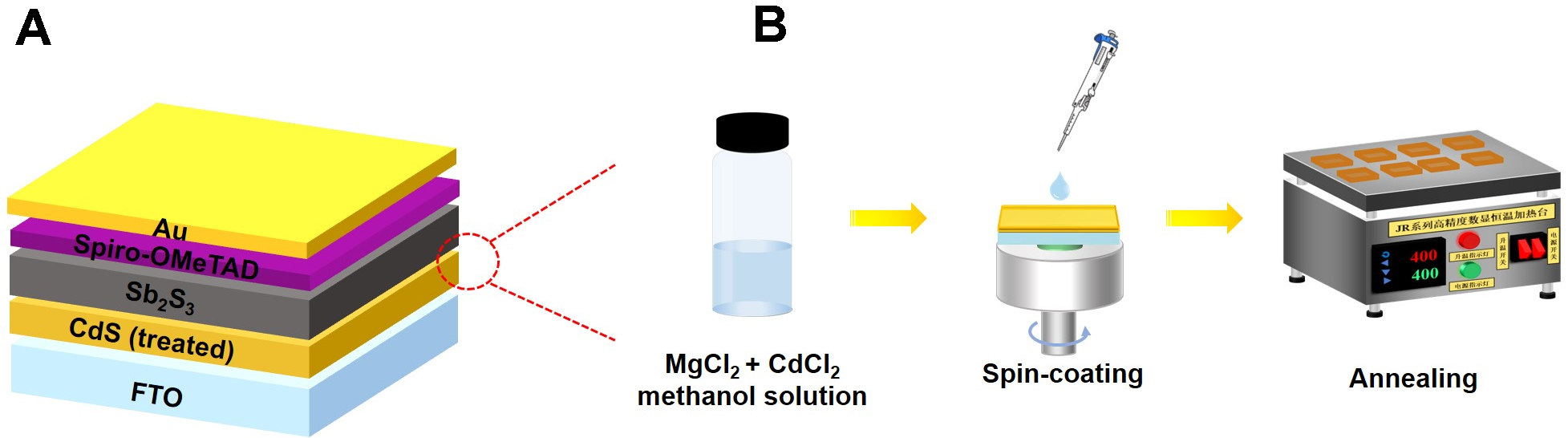
Figure 1. (A) Schematic diagram of the Sb2S3 device structure, (B) Interface processing diagram. CdS: Cadmium sulfide; FTO: fluorine-doped tin oxide.
Currently, the CdCl2 treatment for CdS ETL is a widely applied method in Sb2S3 solar cells. Based on this, we designed four sets of experiments to investigate the treatment effects, including untreated, only CdCl2-treated, only MgCl2-treated, and MgCl2-CdCl2 mixed-treated CdS films. The surface morphologies of the CdS films under the different treatments are characterized by an SEM and shown in Figure 2A-D. Compared to the traditional CdCl2-treated film, the MgCl2-CdCl2 mixed-treated (named MgCl2-M-treated) CdS film exhibits a flatter and denser surface morphology, which facilitates the uniform deposition of the Sb2S3 absorber layer for a dense heterojunction interface. Subsequently, the Sb2S3 thin films are deposited on the above CdS films, as shown in Figure 2E-H. The without (w/o) treated Sb2S3 film exhibits significantly smaller grain sizes, along with a high density of surface pinholes and particle accumulations that serve as effective trap centers, as demonstrated in Figure 2E. Although CdCl2-treated Sb2S3 films exhibit fewer surface particulates and larger grain sizes [Figure 2F], residual pinholes facilitate unintended contact between the hole transport layer and the Sb2S3 film. The Mg2+ introduction makes the CdS film much denser and promotes the crystallization of the absorber layer [Figure 2G]. In contrast, the Sb2S3 film deposited after MgCl2-M treatment exhibits significantly larger grain sizes, higher film density, and reduced pinhole counts [Figure 2H]. Larger grain sizes typically imply fewer grain boundaries[26], which helps reduce the probability of non-radiative recombination at grain boundaries and improves carrier transport properties within the absorber layer. Grazing-incidence X-ray diffraction (GIXRD) characterization is performed on the CdS film under the aforementioned conditions to investigate the influence of MgCl2-M treatment on the crystal structure and orientation. As shown in Figure 2I, all the CdCl2, MgCl2, and MgCl2-M treated CdS films display a mixed structure of cubic and hexagonal phases, with diffraction peaks corresponding to the (100), (111), and (101) crystal planes in ascending order of diffraction angle, while the untreated CdS film only shows a cubic structure. According to literature reports[11,27], the (100) crystal plane of the CdS film is non-polar, which is favorable for Sb2S3 bonding on the CdS film, promoting the vertical growth of (Sb4S6)n bands along the [hk1] direction (h, k = 0, 1, 2...), which is beneficial for carrier transport between bands. The XRD characterizations of the above Sb2S3 films are shown in Figure 2J. For ease of comparison, the peaks are normalized. It is clearly observed that the diffraction peak intensities of the (211) and (221) crystal planes are significantly enhanced. This indicates that MgCl2-M treatment promotes the vertical growth of Sb2S3 film and enhances the carrier transport ability.
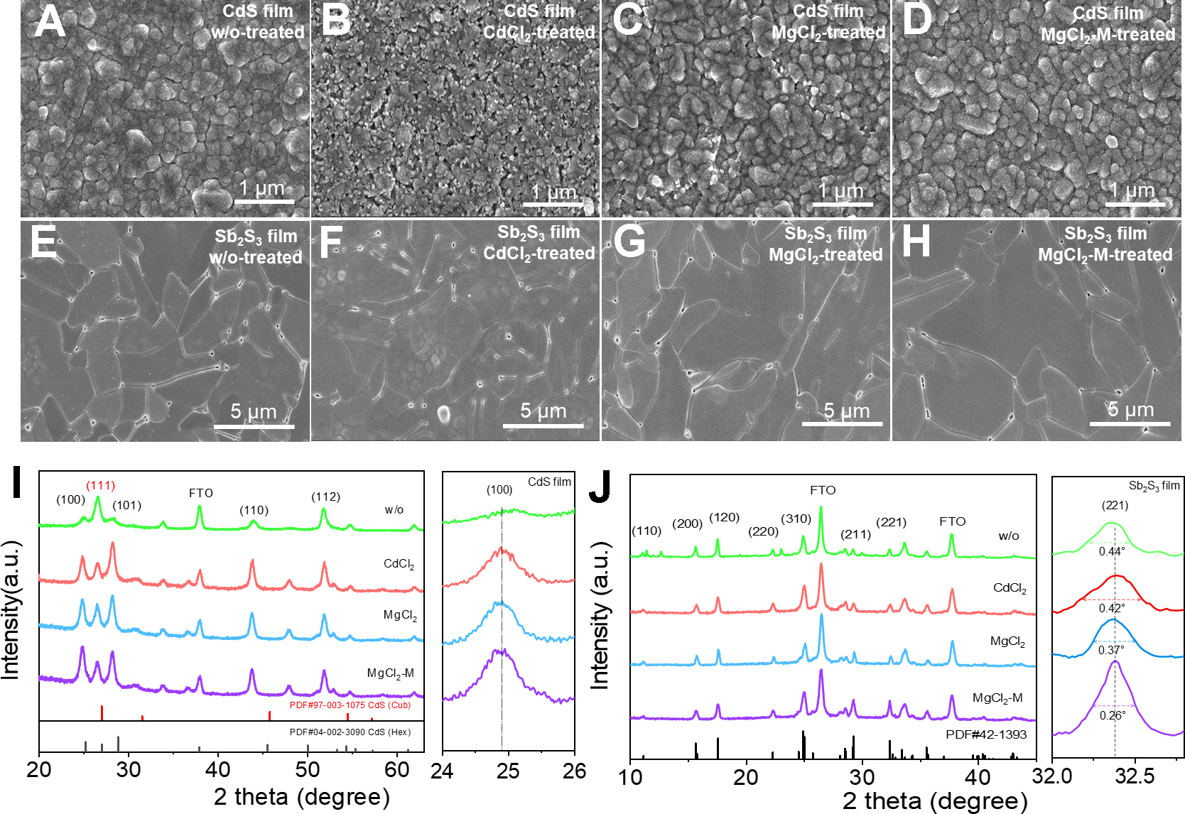
Figure 2. (A-D) SEM images of the CdS films, (E-H) SEM images of the Sb2S3 films, (I) GIXRD diffraction patterns of the CdS films, (J) XRD diffraction patterns of the Sb2S3 films. CdS: Cadmium sulfide; SEM: scanning electron microscope; GIXRD: grazing-incidence X-ray diffraction; XRD: X-ray diffraction.
Sb2S3 thin-film solar cells in the configuration of FTO/CdS(treated)/Sb2S3/Spiro-OMeTAD/Au are constructed to evaluate the impact of MgCl2-CdCl2 mixed-treatment on performance. The statistical distributions of the VOC, short-circuit current density (JSC), FF, and PCE of the solar cells are presented in Figures 3A-D. The untreated device exhibits a VOC of 0.723 V, a JSC of 15.5 mA cm-2, and a FF of 58.1%, resulting in a PCE of 6.51%. Compared to the untreated devices, the performance of devices using other processing methods has been significantly enhanced in VOC and FF, with the most pronounced enhancement observed under MgCl2-M treatment conditions. Figure 3E displays the J-V curves of the w/o, CdCl2, MgCl2, and MgCl2-M treated devices under the standard air mass (AM) 1.5G light illumination. And the corresponding photovoltaic parameters are shown in Table 1. The MgCl2-M device exhibits a VOC of 0.777 V with 7.6% enhancement, a JSC of 16.7 mA cm-2, and a FF of 62.7% with 7.9% increment, resulting in a PCE of 8.1%. Compared with the related halide post-treatments interface (such as SbCl3, PbCl2, NaF)[21-23], the introduction of Mg2+ from MgCl2 can control the bandgap of CdS film, energy band alignments, and interfacial defects, which exhibits competitive potential in increasement of VOC and FF. Subsequently, we further characterize the EQE of these devices [Figure 3F]. The wavelength range for the EQE response of the Sb2S3 device is 300-780 nm. The MgCl2-M device demonstrates the highest photo response (up to 90%) in the range of 300-780 nm. MgCl2-M treatment effectively suppresses parasitic absorption in the CdS layer (within the 300-500 nm wavelength range), improving the utilization of incident sunlight. Additionally, the EQE spectrum in 600-780 nm has also improved slightly, which is attributed to the improved quality of the Sb2S3 film. According to the EQE spectra, the integrated current densities of the w/o, CdCl2, MgCl2, and MgCl2-M devices are calculated, which are consistent with the JSC values obtained from the J-V curves.
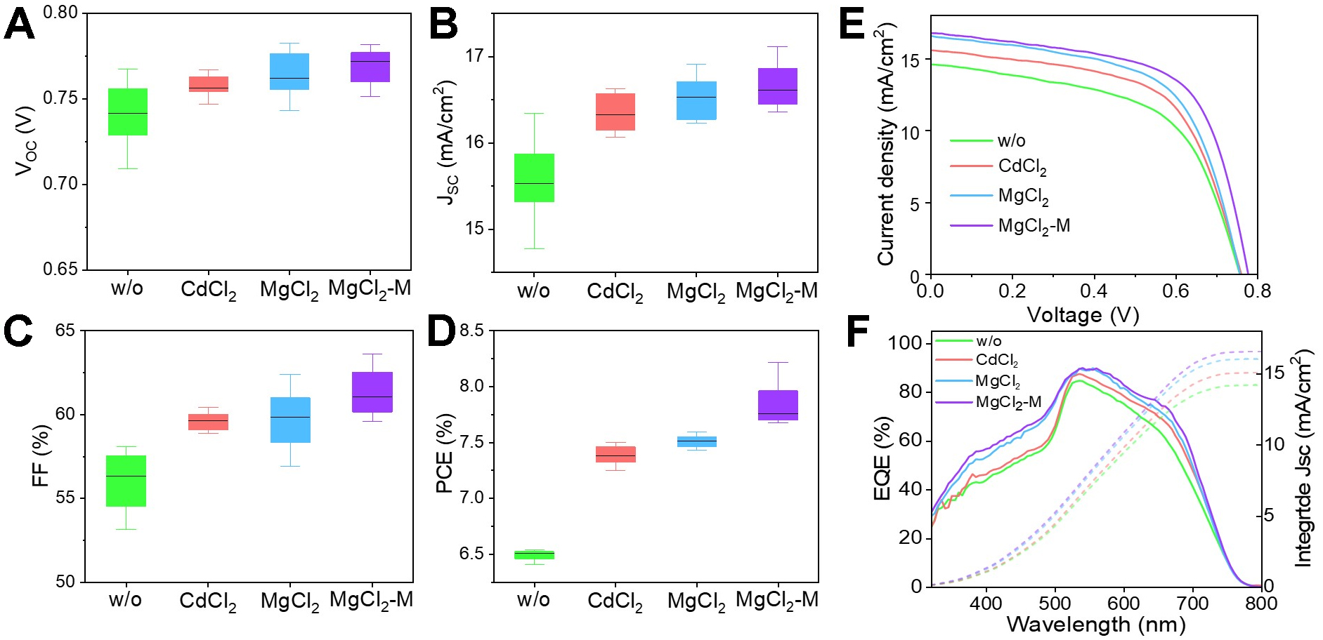
Figure 3. Photoelectric performance of the Sb2S3 solar cells. Statistical distribution of photovoltaic parameters for different treatment methods, including (A) VOC, (B) JSC, (C) FF, and (D) PCE; (E) J-V curves and (F) EQE spectra. VOC: Open-circuit voltage; JSC: short-circuit current density; FF: fill factor; PCE: power conversion efficiency; J-V: current density-voltage; EQE: external quantum efficiency.
Photovoltaic parameters of the champion Sb2S3 devices
| Devices | VOC (V) | JSC (mA/cm2) | FF (%) | PCE (%) |
| w/o | 0.723 | 15.5 | 58.1 | 6.5 |
| CdCl2 | 0.757 | 16.5 | 60.3 | 7.5 |
| MgCl2 | 0.762 | 16.3 | 61.3 | 7.6 |
| MgCl2-M | 0.777 | 16.7 | 62.7 | 8.1 |
Considering the widespread use of CdCl2 treatment, the following discussion focuses exclusively on a comparative study of CdCl2 and MgCl2-M treatments. The XPS is employed to analyze changes in elemental composition and chemical states in CdCl2 and MgCl2-M treated CdS layers [Figure 4A-C and Supplementary Figure 3]. The XPS spectra of all samples were calibrated using the C 1s peak at 284.8 eV as the binding energy reference. High-resolution spectra in the core-level regions, such as Cd 3d, S 2p, and Mg 2p, are deconvoluted to extract chemical state information of the relevant elements. The XPS spectrum of the MgCl2-CdCl2 mixed-treated sample [Figure 4A] clearly shows the characteristic Mg peak at 50.9 eV, which is absent in the control spectrum. This observation indicates successful Mg incorporation into the CdS buffer layer. Figure 4B presents the Cd 3d spectrum of the control CdS, with characteristic peaks at 405.2 eV
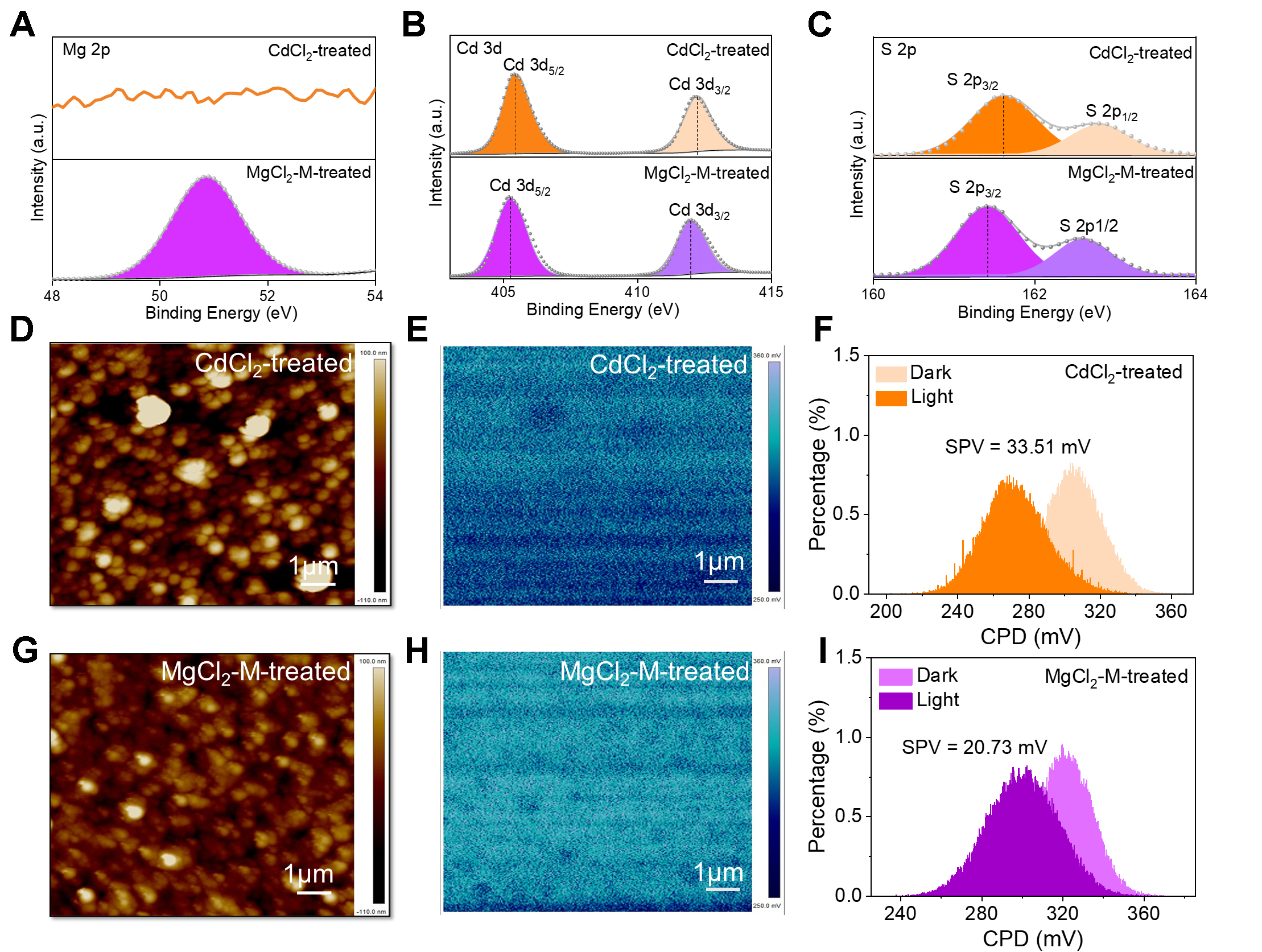
Figure 4. XPS spectra of (A) Mg 2p, (B) Cd 3d, and (C) S 2p. (D) and (G) AFM images; (E) and (H) KPFM images; (F) and (I) statistical potential distributions of CdCl2 and MgCl2-M treated CdS films. XPS: X-ray photoelectron spectroscopy; KPFM: Kelvin probe force microscopy; CdS: cadmium sulfide; SPV: surface photovoltage; AFM: atomic force microscope.
The surface morphology evolution and potential distribution are characterized by KPFM and shown in Figure 4D-F (CdCl2-treated CdS sample) and Figure 4G-I (MgCl2-M treated CdS sample). Compared to the surface roughness (43.7 nm) of the CdCl2-treated CdS film (see Figure 4D), the mixed-treated CdS film exhibits a reduced roughness of 22.6 nm (see Figure 4G). This improved surface smoothness facilitates more homogeneous deposition of the subsequent Sb2S3 absorber layer, thereby enabling the formation of a flatter and better-defined heterojunction interface. The MgCl2-M-treated CdS film exhibits higher and more uniformly distributed contact potential difference (CPD) values [Figure 4E and H]. This increase in VCPD indicates a lower work function for the treated CdS, meaning its Fermi level (EF) is closer to the vacuum level[28]. Within the CdS/Sb2S3 heterojunction architecture, this upward shift of the EF in the CdS layer enhances quasi-EF splitting, leading to an increased built-in potential (Vbi). This enhancement is a key factor contributing to the improvement in VOC. The magnitude of surface photovoltage (SPV) is commonly associated with the surface defect density of semiconductor materials[29]. To further evaluate the influence of MgCl2-M treatment on CdS film surface defect states, the CPD changes under dark and illuminated conditions are measured, as shown in Figure 4F and I. The CdCl2-treated CdS film exhibits an SPV of
The band gap, band structure, and charge-transfer characteristics of the devices are used to determine interfacial energy-level alignments. As shown in the ultraviolet-visible absorption spectra (see Supplementary Figure 4A), the MgCl2-M-treated CdS film exhibits reduced absorption in the 300-500 nm region, thereby minimizing absorption losses. This enhanced optical transparency promotes greater photon transmission to the underlying Sb2S3 absorber layer. The fitted optical bandgaps of CdCl2-treated and MgCl2-M-treated CdS films are 2.39 and 2.38 eV, respectively [Supplementary Figure 4B and C]. The band gaps of the corresponding Sb2S3 films are the same 1.73 eV [Supplementary Figure 5], which is not affected by interface treatment. Furthermore, UPS is used to elucidate the regulatory mechanism of MgCl2-M treatment on the carrier dynamics of the Sb2S3 device. UPS can characterize the electronic structure of valence-band electrons and determine the EF and the valence-band position of a material by analyzing the cutoff edge and the Fermi edge[30]. Figure 5A-D presents the UPS spectra of CdS and Sb2S3 films under distinct treatment conditions. According to the cutoff edges (17.01 eV) and Fermi edges (2.08 eV) in Figure 5A, the calculated conduction band and valence band of the CdCl2-treated CdS film are -3.9 and -6.29 eV, respectively. The conduction band and valence band of the MgCl2-M-treated CdS film are -3.82 and -6.2 eV, respectively (see Figure 5B). The EF of the CdS film shifts upward from -4.21 eV to -4.14 eV, reflecting an increased carrier concentration and enhanced electron collection. In addition, the calculated conduction bands of the two Sb2S3 films are -3.7 and -3.92 eV, and the valence bands are -5.43 and -5.65 eV, respectively [Figure 5C and D]. Based on these results, the band structure alignments at the CdS/Sb2S3 interface after CdCl2 and MgCl2-M treatment are shown in Figure 5E and F, respectively. The conduction band offset (CBO, ΔEC) of the common CdCl2-treated CdS/Sb2S3 interface is 0.2 eV, presenting a cliff-type alignment. Under this condition, electrons in the CdS conduction band readily transition to the valence band of Sb2S3, resulting in recombination. The MgCl2-M treatment significantly modifies the energy level position of the conduction band. The CBO narrowed to -0.1 eV forms a spike-like energy band alignment, which reduces the back-contact barrier and enhances charge separation efficiency. Furthermore, it reduces the device’s reverse saturation current and directly increases VOC.
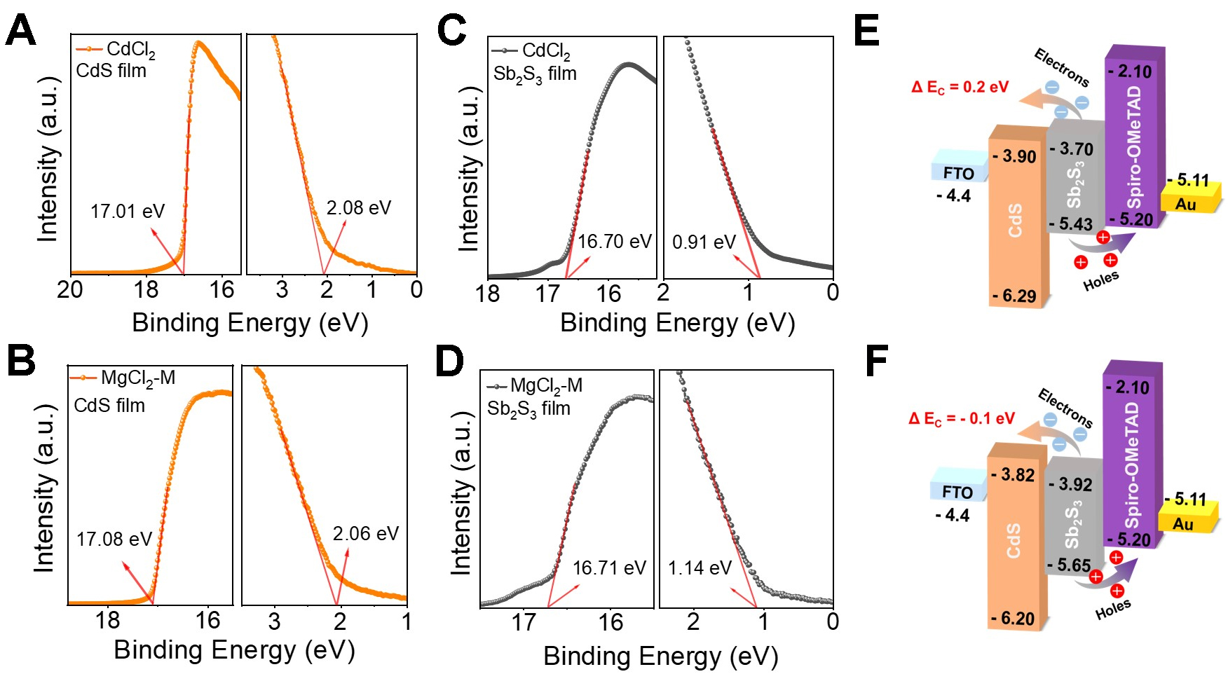
Figure 5. XPS spectra of (A) CdCl2-treated and (B) MgCl2-M-treated CdS films; XPS spectra of Sb2S3 films on (C) CdCl2-treated and (D) MgCl2-M-treated CdS films. Energy level diagrams of (E) the CdCl2 and (F) MgCl2-M treated the device. XPS: X-ray photoelectron spectroscopy; CdS: cadmium sulfide; FTO: fluorine-doped tin oxide.
Carrier transport and collection characteristics are measured to probe the physical mechanism. The dark J-V measurements of the CdCl2 and MgCl2-M treated devices are presented in Figure 6A. Both the Sb2S3 devices exhibit good rectifying behavior. Notably, the MgCl2-M-treated device displays a substantially lower reverse saturation current density (J0) compared to the CdCl2-treated device [Supplementary Figure 6], indicating suppressed leakage pathways, due to reduced defect density and improved junction quality[31]. The ideal factor (A) of the MgCl2-M-treated Sb2S3 device decreases significantly from 2.64 to 1.98. This parameter evolution indicates that MgCl2-M treatment effectively suppresses non-radiative recombination and leakage current paths, significantly improving the quality of the CdS/Sb2S3 heterojunction interface, thereby reducing VOC loss. The Vbi changes are quantified using the capacitance characteristic by the C-2-V curve (see Figure 6B). The Vbi of the device after MgCl2-M treatment increases from 1.17 V to 1.31 V. The enhanced built-in electric field improves carrier separation and transport at the CdS/Sb2S3 heterojunction interface, enabling VOC improvement. Furthermore, EIS also corroborates the above conclusions, with characterization conducted under dark conditions. Figure 6C shows the Nyquist plots for the two devices. Significantly, after MgCl2-M treatment, the recombination resistance (Rrec) increases from 8.3 kΩ to 28.6 kΩ. By applying a gradually increasing forward bias from 0 to 0.4 V, the trend of Rrec of the devices with the bias voltage is displayed in Supplementary Figure 7. The MgCl2-M treated device exhibits remarkably larger impedance magnitudes across and Rrec all the tested bias voltages compared to the control sample, manifesting weaker interfacial carrier recombination and better interface quality[17]. These results indicate that the MgCl2-CdCl2 mixed treatment effectively reduces the charge transfer barrier, promoting carrier separation and transport, thereby enhancing device performance.
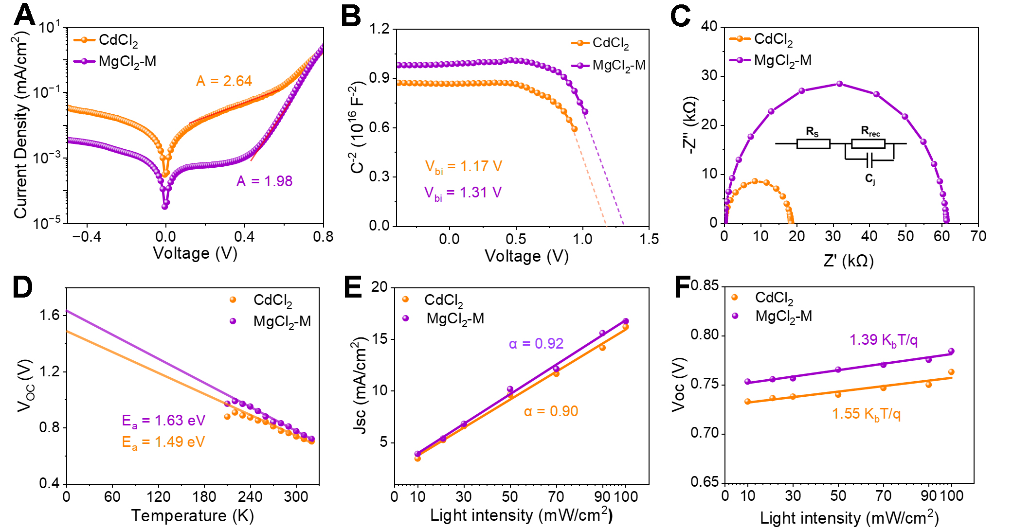
Figure 6. (A) Dark J-V characteristics; (B) 1/C2-V plot; (C) Nyquist EIS curve of CdCl2 and MgCl2-M treated films; (D) Temperature-dependent open-circuit voltage (VOC-T) measurement; Light intensity dependent curves for (E) JSC and (F) VOC. VOC: Open-circuit voltage; JSC: short-circuit current density; J-V: current density-voltage; EIS: electrochemical impedance spectroscopy.
Temperature-dependent J-V characterizations are used to calculate the Ea and analyze the defect recombination mechanism (see Supplementary Figure 8). By fitting the linear segment of the VOC-T curve, the Ea at 0 K is obtained, as shown in Figure 6D. At 0 K, defects within the material are frozen, and electrons occupy the lowest energy levels[32]. The VOC limit is exactly equal to the bandgap. However, when interfacial defects are present, the Ea becomes smaller than the bandgap. The obtained Ea values of CdCl2 and MgCl2-M treated devices are 1.49 and 1.63 eV, respectively. The larger Ea of MgCl2-M device indicates that interfacial defects of CdS/Sb2S3 are significantly passivated compared with the CdCl2-treated device. Meanwhile, the Ea value of the mixed-treated device (1.63 eV) is in proximity to the bandgap of Sb2S3 (1.73 eV), suggesting an extremely low density of interface defects. To further understand the interface carrier recombination and transport characteristics of Sb2S3 devices, light intensity (I) dependent JSC and VOC relationships are analyzed and shown in Figure 6E and F, respectively. The JSC-I curve follows the power-law principle Jsc ∝ Iα, where α is less than 1 due to the space charge effect. The α values for the CdCl2-treated and MgCl2-M-treated devices are 0.90 and 0.92, respectively. A larger α indicates fewer carrier recombination in the MgCl2-M-treated device. Additionally, the relationship between Voc and I can be expressed as Voc = nkbT/qln(I)[33], where kb is the Boltzmann constant, T is the temperature and q is elementary charge. Based on the slope of the fitted line, the n values for the control CdCl2 and MgCl2-M treated devices are 1.55 kbT/q and 1.39 kbT/q, respectively. In principle, this relationship indicates a defect-mediated Shockley-Read-Hall recombination mechanism[34], with slope n values between 1 and 2, indicating that recombination occurs both at the interface and in the bulk material of the device[15]. These results suggest that trap-assisted recombination processes are effectively suppressed in the MgCl2-M-treated devices, consistent with the observed improvements in PCE and FF.
CONCLUSIONS
In summary, we develop a MgCl2-CdCl2 mixed interfacial treatment, enabling bidirectional optimization of the CdS/Sb2S3 heterojunction interface for efficient Sb2S3 thin film solar cells. This treatment effectively reduces parasitic absorption of the CdS film in the short-wavelength (300-500 nm) range, thereby enhancing the photon-harvesting efficiency of the absorber. Additionally, the improved surface quality of the CdS film enables the deposited Sb2S3 film to exhibit a significantly larger grain size, thereby reducing defects. Compared to the conventional CdCl2-treated CdS film, the MgCl2-CdCl2 mixed treatment introduces Mg2+ doping in the CdS layer, adjusting the interfacial energy band alignments. The enhanced surface potential and reduced SPV of the CdS film suppress surface defects. The CdS/Sb2S3 heterojunction interface achieves a transform from “cliff” to “spike” energy band structure and a small CBO (-0.1 eV), improving carrier separation efficiency. Based on these synergistic effects, the MgCl2-M device with a smaller J0 and a large Vbi reveals a high-quality heterojunction. By temperature-dependent VOC characterization, the optimal device Ea of 1.63 eV approaches the bandgap, resulting in effective suppression of nonradiative recombination. The champion Sb2S3 solar cell based on MgCl2-CdCl2 mixed treatment achieves a PCE of 8.1%, with a VOC of
DECLARATIONS
Author contributions
Conceived the study and designed the experiments, device fabrication, and measurement methods: Deng, H.; Liu, Y.; Cheng, S.
Carried out the device fabrication and optimizations: Liu, Y.
Contributed to material characterizations, measurements, and data analysis: Liu, Y.; Peng, C.; Zhu, Q.; Wang, W.
Participated in manuscript discussions, revisions, and data interpretation: Cheng, S.; Wu, J.; Lai, Y.; Lin, P.
Primarily wrote and revised the manuscript: Liu, Y.; Deng, H.
All authors discussed the results and provided critical feedback on the manuscript.
Availability of data and materials
The data that support the findings of this study are available from the corresponding author upon reasonable request.
Financial support and sponsorship
This work was supported by the National Natural Science Foundation of China (Nos. 52372183, 62474043 and 62305064), the Fujian Provincial Natural Science Foundation of China (No. 2024J09015), and the Foundation of Fuzhou University (XRC-24072).
Conflict of interest
All authors declared that there are no conflicts of interest.
Ethical approval and consent to participate
Not applicable.
Consent for publication
Not applicable.
Copyright
© The Author(s) 2026.
Supplementary Materials
REFERENCES
1. Gu, S.; Ullah, S.; Khan, F.; et al. Recent advances and perspectives on Sb2S3 thin-film solar cells. Mater. Today. Sustain. 2024, 28, 101019.
2. Chen, J.; Li, G.; Xu, Z.; et al. Recent Advances and prospects of solution‐processed efficient Sb2S3 solar cells. Adv. Funct. Mater. 2024, 34, 2313676.
3. Chen, X.; Shu, X.; Zhou, J.; et al. Additive engineering for Sb2S3 indoor photovoltaics with efficiency exceeding 17%. Light. Sci. Appl. 2024, 13, 281.
4. Zheng, J.; Liu, C.; Zhang, L.; et al. Enhanced hydrothermal heterogeneous deposition with surfactant additives for efficient Sb2S3 solar cells. Chem. Eng. J. 2022, 446, 136474.
5. Zhong, M.; Wang, X.; Liu, S.; et al. High-performance photodetectors based on Sb2S3 nanowires: wavelength dependence and wide temperature range utilization. Nanoscale 2017, 9, 12364-71.
6. Li, S.; Xu, J.; Shi, S.; Kong, L.; Zhang, X.; Li, L. Self-Powered Ultraviolet-Visible-Near infrared broad spectrum Sb2S3/TiO2 photodetectors and The application in emotion detection. Chem. Eng. J. 2025, 511, 161890.
7. Zhu, J.; Yu, L.; Wang, Z.; et al. High-performance and stable Sb2S3 thin-film photodetectors for potential application in visible light communication. ACS. Appl. Mater. Interfaces. 2023, 15, 28175-83.
8. Shockley, W.; Queisser, H. J. Detailed balance limit of efficiency of p-n junction solar cells. J. Appl. Phys. 1961, 32, 510-9.
9. Shen, G.; Ke, A.; Chen, S.; et al. Strong chelating additive and modified electron transport layer for 8.26%‐efficient Sb2S3 solar cells. Adv. Energy. Mater. 2025, 15, 2406051.
10. Jin, X.; Fang, Y.; Salim, T.; et al. In situ growth of [hk1]‐oriented Sb2S3 for solution‐processed planar heterojunction solar cell with 6.4% efficiency. Adv. Funct. Mater. 2020, 30, 2002887.
11. Li, J.; Xiong, L.; Hu, X.; et al. Manipulating the morphology of CdS/Sb2S3 heterojunction using a Mg-doped tin oxide buffer layer for highly efficient solar cells. J. Energy. Chem. 2022, 66, 374-81.
12. Shah, U. A.; Chen, S.; Khalaf, G. M. G.; Jin, Z.; Song, H. Wide bandgap Sb2S3 solar cells. Adv. Funct. Mater. 2021, 31, 2100265.
13. Myagmarsereejid, P.; Ingram, M.; Batmunkh, M.; Zhong, Y. L. Doping strategies in Sb2S3 thin films for solar cells. Small 2021, 17, 2100241.
14. Deng, H.; Feng, X.; Zhu, Q.; et al. 8.2%-Efficiency hydrothermal Sb2S3 thin film solar cells by two-step RTP annealing strategy. Sci. China. Mater. 2024, 67, 3666-74.
15. Wang, Y.; Yang, D.; Jin, M.; et al. Full‐dimensional penetration strategy with degradable PEAI enables 8.21% efficiency in bulk heterojunction Sb2S3 solar cells. Adv. Energy. Mater. 2025, 15, 2502805.
16. Chen, X.; Zhao, Y.; Li, C.; et al. Interfacial engineering by self‐assembled monolayer for high‐performance Sb2S3 solar cells. Adv. Energy. Mater. 2024, 14, 2400441.
17. Shen, B.; Zhang, T.; Dong, J.; et al. Heterojunction interface anomalous high‐energy level insertion modulating carrier dynamics in high‐efficiency antimony selenide thin‐film solar cells. Adv. Funct. Mater. 2025, 35, 2503922.
18. Liu, R.; Shen, Z.; Zhu, L.; et al. Space-charging interfacial layer by illumination for efficient Sb2S3 bulk-heterojunction solar cells with high open-circuit voltage. ACS. Appl. Mater. Interfaces. 2023, 15, 24583-94.
19. Khallaf, H.; Chai, G.; Lupan, O.; Chow, L.; Park, S.; Schulte, A. Investigation of aluminium and indium in situ doping of chemical bath deposited CdS thin films. J. Phys. D. Appl. Phys. 2008, 41, 185304.
20. Cao, Z.; Shao, B.; Ye, Z.; et al. Anomalous electron doping in CdS to promote the efficiency improvement in Sb2Se3 thin film solar cells. Adv. Funct. Mater. 2025, 35, 2418974.
21. Zhao, Y.; Wang, S.; Jiang, C.; et al. Regulating energy band alignment via alkaline metal fluoride assisted solution post‐treatment enabling Sb2(S,Se)3 solar cells with 10.7% efficiency. Adv. Energy. Mater. 2022, 12, 2103015.
22. Shen, G.; Gao, R.; Chen, S.; et al. Interfacial modification strategy by lead chloride post-treatment enables 8.05% efficient Sb2S3 solar cells. Nano. Research. 2025, 18, 94908031.
23. Cai, H.; Cao, R.; Gao, J.; et al. Interfacial engineering towards enhanced photovoltaic performance of Sb2Se3 solar cell. Adv. Funct. Mater. 2022, 32, 2208243.
24. Wang, L.; Luo, M.; Qin, S.; et al. Ambient CdCl2 treatment on CdS buffer layer for improved performance of Sb2Se3 thin film photovoltaics. Appl. Phys. Lett. 2015, 107, 143902.
25. Su, X.; Li, D.; Xie, Q.; et al. Anion-vacancy defect passivation for efficient antimony selenosulfide solar cells via magnesium chloride post-growth activation. Small 2025, 21, 2412322.
26. Wu, W.; Tang, B.; Wan, L.; et al. Enhanced performance of close-spaced sublimation processed antimony sulfide solar cells via seed-mediated growth. Adv. Sci. 2024, 11, 2409312.
27. Shen, L. Y.; Qin, D. Y.; Nie, E. R.; et al. Fluorine-doped cds enables oriented growth and defect suppression in Sb2Se3 solar cells with high conversion efficiency. Adv. Funct. Mater. 2026, 36, e15011.
28. Ishaq, M.; Li, X.; Mehmood, S.; et al. Heterojunction interface engineering enabling high transmittance and record efficiency in Sb2S3 semitransparent solar cell. Chem. Eng. J. 2024, 501, 157646.
29. Peng, X.; Ma, Z.; He, Z.; et al. Interfacial bridge bonding enables high‐efficiency Sb2(S,Se)3 solar cells with record fill factor exceeding 73%. Adv. Funct. Mater. 2025, 35, 2503314.
30. Cai, J. R.; Huang, Z. H.; Huang, W. Q.; et al. Oxygen-assisted tailoring of evaporated PbS hole transport layer for highly efficient antimony sulfide solar cells. Small 2024, 21, 2407246.
31. Li, H.; Bao, J. N.; Cai, J. R.; et al. Solution-processed multivalent molybdenum oxide tailoring band alignment for efficient Sb2S3 solar cells. Small 2025, 21, e07731.
32. Deng, H.; Zeng, Y.; Ishaq, M.; et al. Quasiepitaxy strategy for efficient full‐inorganic Sb2S3 solar cells. Adv. Funct. Mater. 2019, 29, 1901720.
33. Wang, G.; Feng, L.; Huang, Y.; et al. Boosting efficiency of hydrothermally grown Sb2S3 solar cells via rational sulfur engineering. Adv. Funct. Mater. 2026, 36, e18624.
Cite This Article
How to Cite
Download Citation
Export Citation File:
Type of Import
Tips on Downloading Citation
Citation Manager File Format
Type of Import
Direct Import: When the Direct Import option is selected (the default state), a dialogue box will give you the option to Save or Open the downloaded citation data. Choosing Open will either launch your citation manager or give you a choice of applications with which to use the metadata. The Save option saves the file locally for later use.
Indirect Import: When the Indirect Import option is selected, the metadata is displayed and may be copied and pasted as needed.
About This Article
Copyright

Data & Comments
Data
0


Comments
Comments must be written in English. Spam, offensive content, impersonation, and private information will not be permitted. If any comment is reported and identified as inappropriate content by OAE staff, the comment will be removed without notice. If you have any queries or need any help, please contact us at [email protected].