


fig2
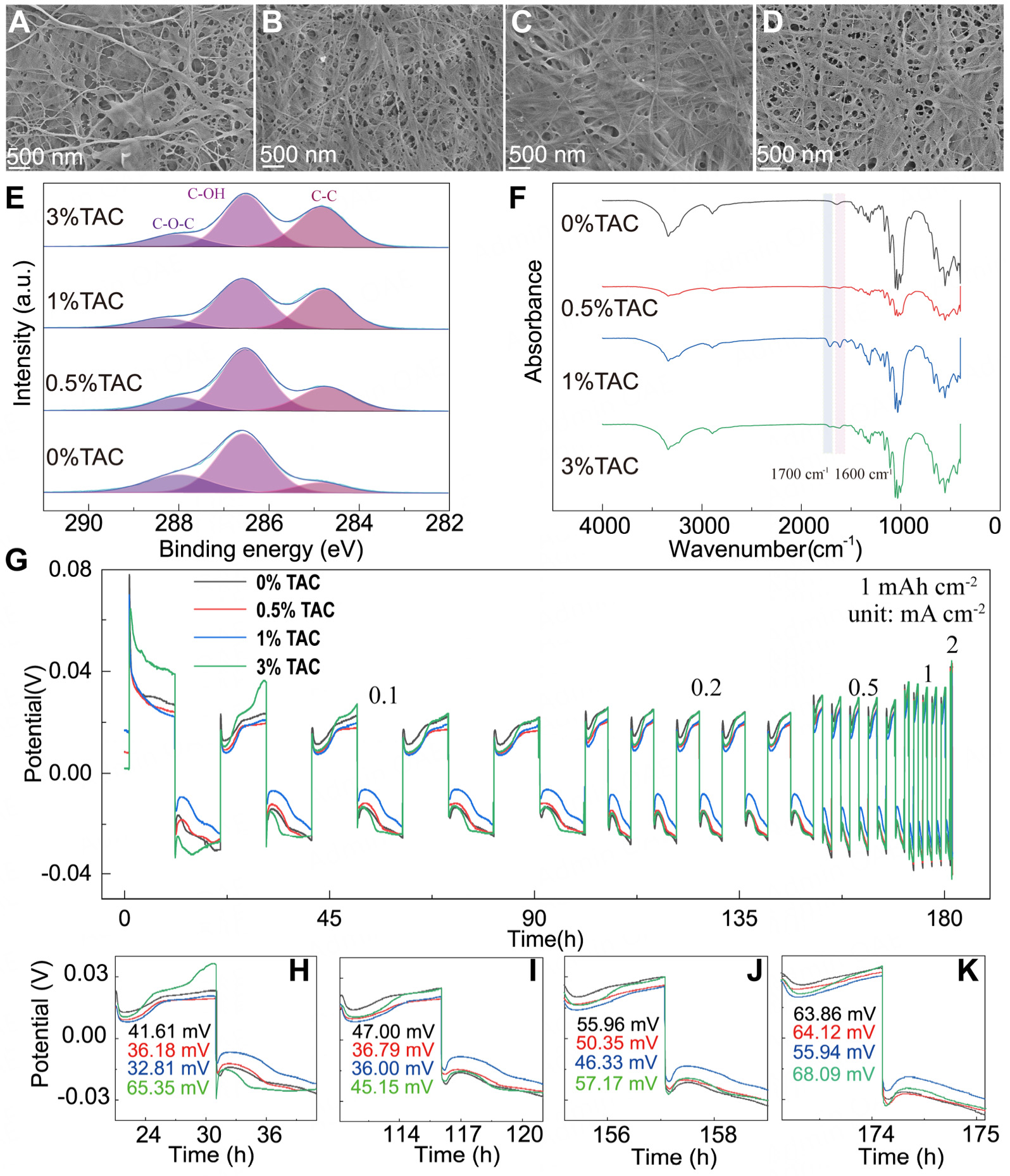
Figure 2. SEM images of (A) 0% TAC, (B) 0.5% TAC, (C) 1% TAC, and (D) 3% TAC; (E) XPS of C 1s of the TAC samples; (F) FTIR spectra of TAC samples; (G) Galvanostatic Zn stripping and plating in a Zn||Zn cell using TAC under different current density (0.1, 0.2, 0.5, 1, and 2 mA cm-2) with 1 mAh cm-2 capacity limitation; Potential profiles of Zn/Zn cell under (H) 0.1, (I) 0.2, (J) 0.5, and (K)


