


fig2
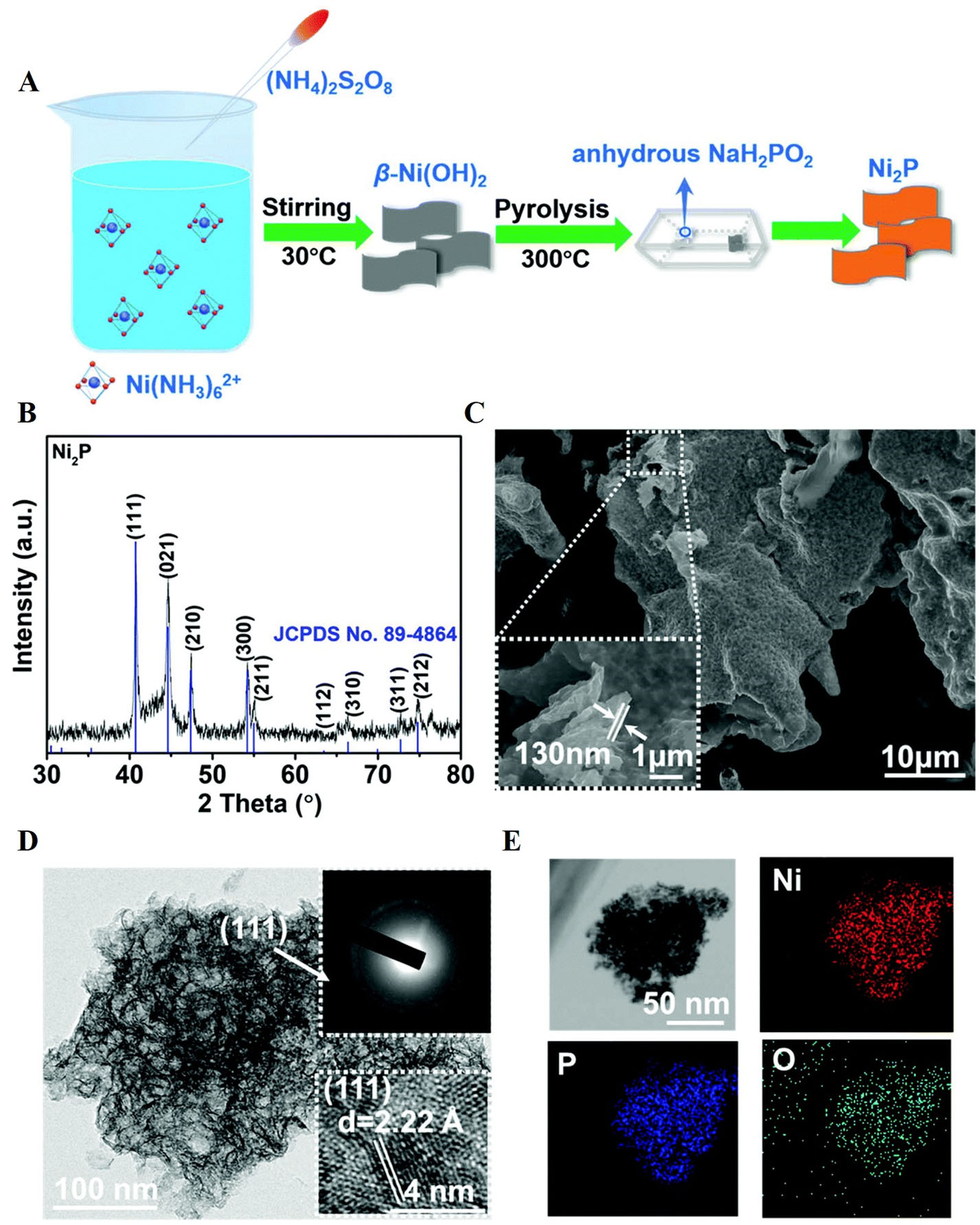
Figure 2. (A) Synthesis of Ni2P nanoflakes; (B) XRD pattern; (C) SEM image; (D) TEM image (inset shows the corresponding HRTEM image and SAED pattern); and (E) STEM-EDS elemental mapping shows uniformity of elemental[100]. This figure is quoted with permission from Liu et al. XRD: X-ray diffraction; SEM: scanning electron microscopy; TEM: transmission electron microscopy; HRTEM: high-resolution TEM; EDS: energy-dispersive X-ray spectroscopy; SAED: selected area electron diffraction.


