

fig1
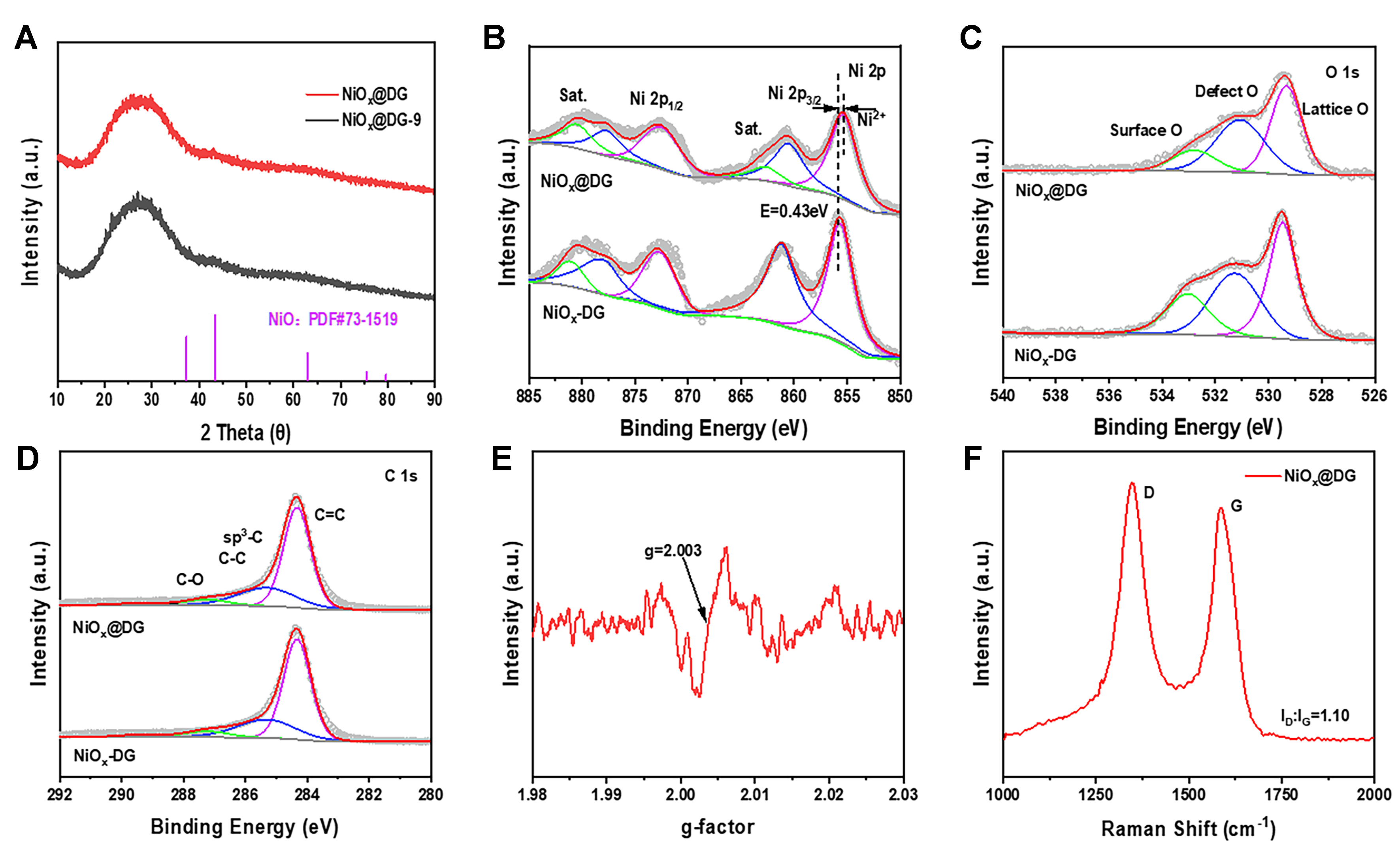
Figure 1. (A) SEM image, (B) TEM image, (C) AFM image of NiOx@DG and (D), Height profile along the line of NiOx@DG; (E) HRTEM image and (F) The enlarged HRTEM image within the red dashed frame marks the local area of disordered atoms; (G and H) SEM and line-scan element mapping for NiOx@DG. SEM: Scanning electron microscopy; TEM: transmission electron microscopy; AFM: atomic force microscopy; DG: defective graphene; HRTEM: high-resolution transmission electron microscopy.